
• Skip to primary navigation
  • Skip to main content
  • Skip to primary sidebar
  • Skip to footer
  • Subscribe
  • Advertise

Power Electronic Tips

Power Electronic News, Editorial, Video and Resources

  • Products
    • Power Supplies
    • AC-DC
    • DC-DC
    • Battery Management
    • Capacitors
    • Magnetics
    • MOSFETS
    • Power Management
    • RF Power
    • Resistors
    • Transformers
    • Transistors
  • Applications
    • 5G
    • AI
    • Automotive
    • EV Engineering
    • LED Lighting
    • Industrial
    • IoT
    • Wireless
  • Learn
    • eBooks / Tech Tips
    • EE Training Days
    • FAQ
    • Learning Center
    • Tech Toolboxes
    • Webinars & Digital Events
  • Resources
    • Design Guide Library
    • Digital Issues
    • Engineering Diversity & Inclusion
    • LEAP Awards
    • Podcasts
    • White Papers
  • Video
    • EE Videos & Interviews
    • Teardown Videos
  • EE Forums
    • EDABoard.com
    • Electro-Tech-Online.com
  • Engineeering Training Days
  • Newsetter Subscription

60 V MOSFET offers RS-S(ON) down to 10 mΩ typical in a 3 mm x 3 mm footprint

December 11, 2019 By Aimee Kalnoskas Leave a Comment

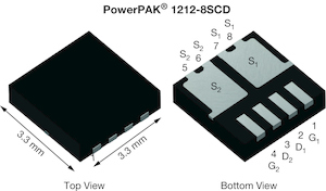
RS-S(ON) Down to 10 mΩ Typical Vishay Intertechnology, Inc. introduced a new common-drain dual n-channel 60 V MOSFET in the compact, thermally enhanced PowerPAK 1212-8SCD package. Designed to increase power density and efficiency in battery management systems, plug-in and wireless chargers, DC/DC converters, and power supplies, the Vishay Siliconix SiSF20DN offers the industry’s lowest RS-S(ON) in a 60 V common-drain device.

The dual MOSFET released today provides RS-S(ON) down to 10 mΩ typical at 10 V, the lowest among 60 V devices in the 3 mm by 3 mm footprint. This value also represents a 42.5 % improvement over the next best solution in this footprint size and is 89 % lower than Vishay’s previous-generation devices. The result is reduced voltage drops across the power path and minimized power losses for increased efficiency. For higher power density, the SiSF20DN’s RS1S2(ON) times area is 46.6 % lower than the next best alternative MOSFET, even when including larger 6 mm by 5 mm solutions.

To save PCB space, reduce component counts, and simplify designs, the device uses an optimized package construction with two monolithically integrated TrenchFET Gen IV n channel MOSFETs in a common drain configuration. The SiSF20DN’s source contacts are placed side by side, with enlarged connections increasing the contact area with the PCB and reducing resistivity further compared to conventional dual package types. This design makes the MOSFET ideal for bidirectional switching in 24 V systems and industrial applications, including factory automation, power tools, drones, motor drives, white goods, robotics, security/surveillance, and smoke alarms.

The SiSF20DN is 100 % Rg- and UIS-tested, RoHS-compliant, and halogen-free.

Samples and production quantities of the new MOSFET are available now, with lead times of 30 weeks for larger orders. Pricing for U.S. delivery only starts at $0.86 per piece in 10,000-piece quantities.
You may also like:

  • MOSFET
    What is the MOSFET body diode?

  • How and when MOSFETs blow up

Filed Under: MOSFETS Tagged With: vishayintertechnology

Reader Interactions

Leave a Reply

You must be logged in to post a comment.

This site uses Akismet to reduce spam. Learn how your comment data is processed.

Primary Sidebar

Featured Contributions

How to design ultra-low-power smart thermostats without a C-wire

Vertical power delivery reduces losses in AI processor designs

Protecting Ethernet interfaces in telecommunications applications against common high energy surges

Ionic cooling: a silent revolution in thermal management

Robust design for Variable Frequency Drives and starters

More Featured Contributions

EE LEARNING CENTER

EE Learning Center

EE TECH TOOLBOX

“ee
Tech Toolbox: Sensors
In this Tech Toolbox, we cover some of those technologies driving the next generation of connected systems, including ultra-low-power sensing strategies that extend node battery life, and 60 GHz CMOS radar for contactless health and presence detection.

EE ENGINEERING TRAINING DAYS

engineering
“power
EXPAND YOUR KNOWLEDGE AND STAY CONNECTED
Get the latest info on technologies, tools and strategies for EE professionals.
“bills

RSS Current EDABoard.com discussions

RSS Current Electro-Tech-Online.com Discussions

  • Difference between TTL, RS232 and RS485
  • Beginner Questions About CNC Machines – G-code, Control Systems & Accuracy
  • Smart Buoy project
  • Need Guidance to reduce noise in 3-stage Transimpedance amplifier
  • Wall Radiator Heating: Efficiency and Placement Questions

Footer

EE World Online Network

  • 5G Technology World
  • EE World Online
  • Engineers Garage
  • Analog IC Tips
  • Battery Power Tips
  • Connector Tips
  • EDA Board Forums
  • Electro Tech Online Forums
  • EV Engineering
  • Microcontroller Tips
  • Sensor Tips
  • Test and Measurement Tips

Power Electronic Tips

  • Subscribe to our newsletter
  • Advertise with us
  • Contact us
  • About us

Copyright © 2026 · WTWH Media LLC and its licensors. All rights reserved.
The material on this site may not be reproduced, distributed, transmitted, cached or otherwise used, except with the prior written permission of WTWH Media.

Privacy Policy