
Converters with built-in holdup circuitry reduce the size and requirements for input capacitors.
Dr. André Buffing, L. Dinkelmann, Traco Power
DC/DC converters are generally designed to maintain their output despite brief interruptions of their input power. The duration of this output hold-up often is set by the value of an external capacitor connected across the converter input terminals. However, some types of converters now feature a dedicated holdup capacitor connection (Bus pin). This scheme can save up to 93% on external capacitor costs while reducing their volume by up to 93% as well.
A case study helps illustrate the benefits of the approach. Consider as an example the power supply for a passenger information system as used on (light) rail vehicles. Light rail applications can experience long supply voltage interruptions. The EN 50155 standard for railway applications – rolling stock spells out requirements for the operation, design, and testing of electronic equipment on rail vehicles. Thanks to its comprehensive consideration of “harsh” environmental conditions, the EN 50155 is often considered for design of ruggedized industrial applications. This includes continued operation during an interruption of the supply voltage for a duration of up to 20 msec, a common occurrence in battery powered applications.
During the interruption, the input may be shorted. Power must come from an (external) hold-up capacitor bank. The design of the holdup circuit and the dimensioning of the capacitor bank are important parts of the overall application design process.
Light rail passenger information systems typically include a small screen, a field computer and networking peripherals such as industrial ethernet and/or IEEE 802.11 wireless communication. A 40-W power supply is typically adequate for handling these demands. Important electrical requirements of the dc supply include providing the industry standard 24, 48, 96, and 110-V battery system voltages as well as high and low input voltage limits, a maximum transient input voltage, and the maximum duration of an interruption the supply can handle.
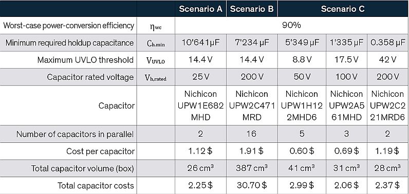
We’ll consider three scenarios involving three different holdup circuits. Scenario A presents the use of a supply which also contains a dedicated holdup capacitor connection. Scenario B uses a comparable 12:1 ultra-wide input voltage range product which does not include a dedicated low-voltage holdup capacitor circuit. Scenario C presents a reference design based on a state-of-the-art 4:1 wide input voltage range dc/dc converter which also does not incorporate a dedicated holdup capacitor connection.
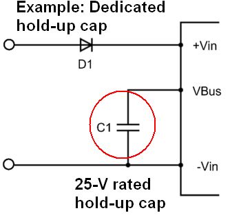
The sizing of the holdup capacitor bank differs for all three scenarios. In scenario A, normal operation charges the holdup capacitor through an internal circuit of the dc/dc converter. If there is an interruption in the supply voltage, the dedicated holdup circuit automatically switches the power over from the input clamps to the external holdup capacitor. A diode in the input of the dc/dc converter prevents an accidental reversal of the supply voltage from damaging the converter and prevents the hold-up capacitor bank from discharging into the main power source.
The minimum holdup capacitance C1 = Ch,min is calculated according to
![]()
where ηwc = dc/dc converter power conversion efficiency at full load, Vuvlo = the lowest input voltage at which the converter can operate properly, Vh,nom = the charge voltage of the holdup capacitance during normal operation, Pnom = dc/dc converter nominal power, and Thold = holdup time, seconds. A factor of 1.5 is included to account for component tolerances and other non-idealities.
Thanks to the extended holdup feature, Vh,nom is a constant 21.4 V for all nominal input voltages during normal operation. This allows the application designer to use low-voltage capacitors for the holdup energy storage with a Vc1,rated rated voltage of 25 V. The fact that Vc1,rated is only slightly above Vh,nom underlines the effectiveness of the design. The holdup time can be reached even if an interruption occurs at the lowest nominal voltage, as required by the EN 50155.
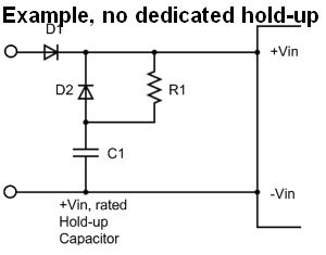
Scenario B employs a dc/dc converter input circuit that contains the holdup capacitor, two diodes, and a resistor R1. During normal operation, the holdup capacitor charges via the resistor. In case of a supply voltage interruption, the holdup capacitor supplies its stored energy to the dc/dc converter via one of the diodes. The other diode prevents converter damage in case of an accidental reversal of the input voltage.
The selection of R1 presents a trade-off between limiting the inrush current and minimizing the (re-)charge time of the capacitor bank. The minimum holdup capacitance C2 = Ch,min is calculated according to
![]()
where the variables represent the same entities as in equation one. Because there is no dedicated holdup circuit, the holdup capacitor voltage Vh,nom follows the input voltage, thus Vh,nom = Vnom,min = 24 V. The capacitor bank must be designed for the maximum (transient) input voltage of Vh,rated ≥Vin,max ≥154 V. The need to handle a high input voltage presents a significant drawback for the conventional design. To provide a cushion for safe operation, a Vh,rated of 200 V might be specified.
Turning to scenario 3, dc/dc converters with a 12:1 ultra-wide input voltage range have come to market only recently. So we will consider a state-of-the-art design using a dc/dc converter with a 4:1 wide input voltage range. The limited input voltage range forces the use three different dc/dc converters, one for each nominal system voltage. But the design methodology for the holdup circuits is virtually identical to that in scenario B.
Test results
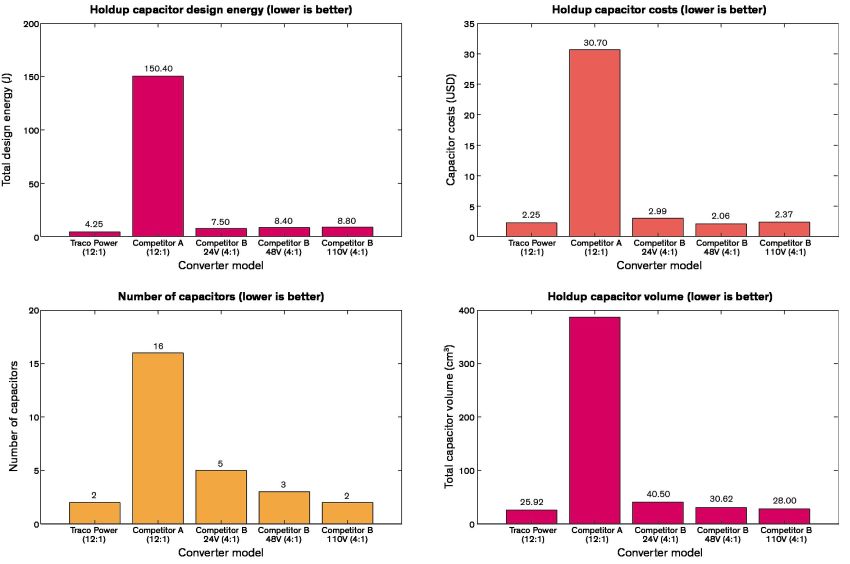

All in all, when using a converter like that in scenario A, such as the Traco Power TEP 40UIR dc/dc converter, the application engineer can save up to 93% on holdup capacitor costs and reduce the volume of the holdup capacitors by up to 93% compared to an approach without a dedicated holdup circuit. And developers can reduce engineering, certification, testing, assembly, retooling, stocking, maintenance, and support costs as well.


Leave a Reply