
Here’s how a 3D EM simulation can be used to accurately gauge gate-driver trace inductance.
JOHN RICE | TEXAS INSTRUMENTS INC.
HIGH ELECTRON MOBILITY TRANSISTORS (HEMTS) were first introduced in the early 1980s and are touted for their exceptional switching qualities. These so-called heterojunction, field effect transistors (FETs) were originally developed for high-frequency RF power amplifiers. More recently, however, these heterojunction transistors have evolved to address a broader scope of high-frequency, high-voltage and high-current power applications.
Today power transistors built on wide-bandgap (WBG) semiconductor materials including silicon carbide (SiC) and gallium nitride (GaN) are being used to realize higher power efficiency and higher power density at a lower cost. In this regard, 3D electromagnetic (EM) field solvers help isolate and resolve printed circuit board (PCB) and component parasitic coupling that otherwise would compromise the wide bandgap (WBG) transistor advantage.
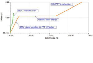
MOSFETs built-in silicon and the latest WBG transistors are both FETs. As such, the turn-on and turn-off behavior is largely a function the device’s composite gate charge. Until the gate-drain “miller capacitance” of the FET is charged, the device remains in a high on-resistance state. The gate driver sources and sinks current into the gate terminal to move up and down the device’s gate charge curve. The rate at which this happens is determined by the driver output current and the device gate charge. It is the ultralow gate charge characteristic of WBG transistors that facilitates high-frequency operation in high-power applications, reducing both power stage and gate driver losses in hard-switch applications.
Also evident from a gate charge curve is that a full saturation of the vertically-structured, super-junction transistor requires nearly twice the gate potential compared with the laterally-structured GaN device. In fact, gate-source voltages exceeding about 6 V can damage some GaN transistors. GaN FETs with a low-voltage gate oxide capability need specialized GaN FET gate drivers like the Texas Instruments LM5113.
As we will see, the key requirement in advancing high-frequency power is to minimize distributed parasitic coupling. To help address this need, TI introduced the LMG3410. This 600-V, 12-A device integrates a gate driver with a depletion-mode (normally on) GaN FET that delivers high-frequency, enhancement-mode switch operation from a logic-level input.
Some GaN manufacturers leverage the ultralow on-resistance of GaN technology by building high-voltage enhancement-mode GaN transistors in a cascode arrangement of a low-voltage silicon MOSFET and high-voltage depletion-mode GaN device. These GaN devices typically exhibit a gate oxide capability comparable to that of silicon MOSFETs.
What to expect with GaN
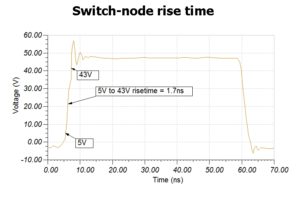
The accompanying figure illustrates the half-bridge switch node behavior of a 48-V-to-1-V buck converter delivering 10 A. At 24 V/nsec, the measured switch node dv/dt is at least ten times faster than what is typically seen with silicon MOSFETs; and yet, GaN technology is capable of even faster dv/dt. Still, the PCB and component parasitics that were benign with silicon MOSFETS often become problematic when using WBG transistors.
Current flow from the gate driver of a power FET is complex. It is affected by dc and ac parasitic impedances including PCB layout copper, component internal inductance, FET capacitances and driver dc resistance. If the gate driver output is overdamped, the GaN advantage will be partially lost. If the gate driver is underdamped, oscillations at the FET gate and switch node can create excessive electromagnetic interference (EMI) and electrical overstress (EOS).
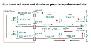
The significant parasitic elements and gate drive current vectors are evident in the nearby figure depicting the of gate/driver distributed impedance and sink/source currents. But it is difficult to quantify the actual circuit behavior when parasitic elements are activated by switch-path di/dt and dv/dt. Note that probing a switch node typically adds between 3 and 20 pF of capacitance and should be considered as an invasive measurement that can mask parasitic behavior. Measurement equipment including scope/probe bandwidth must be considered carefully.
Now consider the parasitic elements of a transmission line. A transmission line is any pair of conductors used to move energy from one point to another. In the case of a MOSFET driver, the transmission line is from the driver decoupling capacitor, CVDD, to the FET gate terminal. It is essential to quantify the distributed impedance to ensure the resonant tank made up of the gate driver, PCB transmission line and the FET gate capacitance is properly damped.
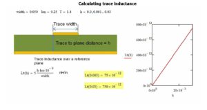
Consider the inductance of a trace as a function of the vertical height, h, above the reference plane. At h = 30 mil above the reference plane, the trace would have about 750 pH of inductance. Reducing the height, h, to 3 mils would result in a proportional reduction of one-tenth the inductance or 75 pH.
Clearly, minimizing stack-up height is essential for reducing PCB trace inductance. Note this first-order approximation does not account for the influence of other material including co-planar copper, copper weight and material dielectric. It takes a finite element analysis (FEA) to precisely analyze the frequency-dependent PCB trace impedance. To solve for the broadband surface-current interaction requires the application of Maxwell’s equations to the finite element mesh.
Fortunately, software and computing power has advanced to the point where this kind of analysis is now possible, even on a laptop computer. More sophisticated analysis will become increasingly important in high-frequency power applications to realize optimal and reliable circuit behavior.
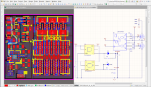
EM simulation tools like CST Microwave Studio can quantify the frequency dependent, parasitic loop inductance in a gate drive circuit. Consider the following example analysis conducted on an Efficient Power Conversion (EPC) EPC920X evaluation module.
The EPC920X half-bridge power stage layout and schematic were both optimized by EPC engineers who are well aware of GaN transistor switching speeds; many designers who want to use GaN technology won’t have the same kind of sensitivities.
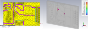
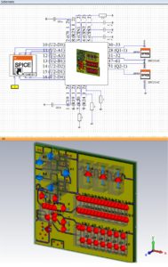
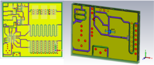
A 3D EM simulation of a PCB section of the PCB helps to precisely calculate the gate drive loop inductance. The analysis here focuses on the interconnect impedance associated with the low-side copper from the gate of Q2 through R24 to the LM5113 gate driver sink pin. The board design was exported from the Altium Designer layout tool as an OBD++ file and imported into CST Microwave Studio. OBD++ files export all physical properties of the board including the layer stack-up. To minimize analysis run-time, we mesh only the relevant portion of a PCB, in this case the low-side gate driver.
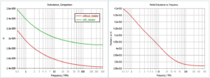
The 3D EM simulation of the section took four minutes to run on a laptop computer with four cores. To calculate partial inductance, we assign current ports to various copper segments of the loop. After meshing and solving the EM coupling mechanisms, we apply a broadband current excitation from 500 kHz to 500 MHz to the gate drive loop to determine the inductance.
The real power of a 3D EM simulator comes into play with an EM analysis of the entire PCB. The board can then be excited within the EM simulator environment using waveforms representative of the application. This “co-simulation” links all the physical coupling mechanisms of the PCB with a circuit-level SPICE analysis. In this way an accurate assessment the board’s high-frequency circuit behavior can be realized.
The learning curve of any simulation tool can be steep; this is especially true with 3D EM simulation. Application of these tools requires a deep understanding of the EM simulator and the end application. If possible, it’s best to pick a tool that has an intuitive user interface, practical application material and excellent technical support. I found all of these at Computer Simulation Technology (CST) and especially appreciated the excellent technical support I received from Patrick DeRoy.
References
Rice, John. Are you accurately measuring the picosecond rise time of your GaN device?, Power House TI E2E Community Blog, July 1, 2015
How to Drive GaN Enhancement Mode Power Switching Transistors, GaN Systems Application note, GN001 Rev 2014-10-21
CST Microwave Studio
Rice, John. Get into electromagnetic compliance with GaN. TI E2E Community Blog, August 26, 2015
Getting Ahead with Coupled 3D Field and Circuit Simulation, Computer Simulation Technology (CST) Webinar
[…] Better high-frequency power design through EM simulation MOSFETs built-in silicon and the latest WBG transistors are both FETs. As such, the turn-on and turn-off behavior is largely a function the device’s composite gate charge. Until the gate-drain “miller capacitance” of the FET is charged, the device remains in a high on-resistance state. […]