• Skip to primary navigation
  • Skip to main content
  • Skip to primary sidebar
  • Skip to footer
  • Subscribe
  • Advertise

Power Electronic Tips

Power Electronic News, Editorial, Video and Resources

  • Products
    • Power Supplies
    • AC-DC
    • DC-DC
    • Battery Management
    • Capacitors
    • Magnetics
    • MOSFETS
    • Power Management
    • RF Power
    • Resistors
    • Transformers
    • Transistors
  • Applications
    • 5G
    • AI
    • Automotive
    • EV Engineering
    • LED Lighting
    • Industrial
    • IoT
    • Wireless
  • Learn
    • eBooks / Tech Tips
    • EE Training Days
    • FAQ
    • Learning Center
    • Tech Toolboxes
    • Webinars & Digital Events
  • Resources
    • Design Guide Library
    • Digital Issues
    • Engineering Diversity & Inclusion
    • LEAP Awards
    • Podcasts
    • White Papers
    • Design Fast
  • Video
    • EE Videos & Interviews
    • Teardown Videos
  • EE Forums
    • EDABoard.com
    • Electro-Tech-Online.com
  • Engineeering Training Days
  • Newsetter Subscription

Current Circuit: A bipolar AC/DC MOSFET low-side switch

November 20, 2016 By Aimee Kalnoskas

by Crutschow, Electro-Tech-Online.com community member

Here’s a circuit that uses two back-to-back N-MOSFETs and one PNP BJT to form a low-side bipolar switch for either AC or plus/minus DC sources. This has much lower On voltage drop and power loss than a TRIAC (for example a Triac will typically dissipate >10W at 10Arms current whereas the two MOSFETs will dissipate a total of <1W for low ON resistance MOSFETs at the same current).

bipolar-circuit-designThe circuit also doesn’t latch on with a DC source as a TRIAC does.
It can be used in place of an SSR when the AC/DC voltage source is already isolated from the Mains by a transformer and thus isolation for the control signal is not required.

The circuit takes advantage of the fact that a MOSFET conducts equally well in both directions when biased ON. Two back-to-back N-MOSFETs are used to allow blocking for both polarities of the supply source (otherwise the parasitic MOSFET substrate diode would conduct in the reverse direction.)

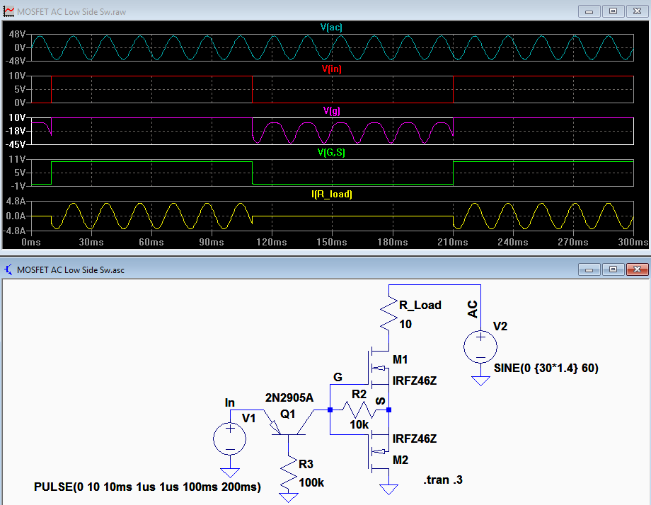
The common-base configured PNP allows the positive control voltage to turn on the MOSFETs, but blocks the negative voltages (Vg, purple trace below) that occur at the gate from the gate-source connection when the control signal is 0V (giving Vg,s = 0V) and the supply voltage goes negative.

The input ON control voltage must be equal to the Vgs voltage for which the ON resistance, Rds(on), is specified in the MOSFET spec sheet. This is typically 10V for standard MOSFETs and 5V (or less) for logic-level type MOSFETs.

The maximum allowed peak AC or DC voltage is determined by the voltage ratings of the MOSFETs and the PNP transistor (whichever is lower). For inductive loads, back-to-back zeners or other transient suppressors will need to be used from the drain of M1 to ground, to limit the peak voltage to at least 25% below the ratings of the transistors.

The LTspice simulation below shows the current through the load resistor R_Load, for high (ON) and zero (OFF) input voltages and a 30Vrms AC source voltage. The ON voltage drop equals the load current times twice the ON resistance of the MOSFET type selected.


For more information about this circuit design go to Electro-Tech-Online.

Filed Under: Featured, Industry Experts Tagged With: electrotechonline.com

Reader Interactions

Comments

  1. Vishal Kakade says

    August 17, 2023 at 2:12 am

    Not Working, FET’s are alays conducting.

Primary Sidebar

Featured Contributions

Meeting demand for hidden wearables via Schottky rectifiers

The case for vehicle 48 V power systems

GaN reliability milestones break through the silicon ceiling

Developing power architecture to support autonomous transportation

What makes SiC tick?

More Featured Contributions

EE LEARNING CENTER

EE Learning Center

EE TECH TOOLBOX

“ee
Tech Toolbox: Internet of Things
Explore practical strategies for minimizing attack surfaces, managing memory efficiently, and securing firmware. Download now to ensure your IoT implementations remain secure, efficient, and future-ready.

EE ENGINEERING TRAINING DAYS

engineering
“power
EXPAND YOUR KNOWLEDGE AND STAY CONNECTED
Get the latest info on technologies, tools and strategies for EE professionals.
“bills

RSS Current EDABoard.com discussions

  • Input impedance matching network
  • Solder Thermal Interface Material
  • Is it possible to improve accuarcy of ad633
  • Unity Gain Buffer with 0 to 0.5V Range
  • Battery sensing circuitry for coin cell application

RSS Current Electro-Tech-Online.com Discussions

  • Trail camera
  • how to work on pcbs that are thick
  • can a AT89C51 be used as a rom?
  • Telegram Based Alarm - Sensor cable protection
  • using a RTC in SF basic

DesignFast

Component Selection Made Simple.

Try it Today
design fast globle

Footer

EE World Online Network

  • 5G Technology World
  • EE World Online
  • Engineers Garage
  • Analog IC Tips
  • Battery Power Tips
  • Connector Tips
  • DesignFast
  • EDA Board Forums
  • Electro Tech Online Forums
  • EV Engineering
  • Microcontroller Tips
  • Sensor Tips
  • Test and Measurement Tips

Power Electronic Tips

  • Subscribe to our newsletter
  • Advertise with us
  • Contact us
  • About us

Copyright © 2025 · WTWH Media LLC and its licensors. All rights reserved.
The material on this site may not be reproduced, distributed, transmitted, cached or otherwise used, except with the prior written permission of WTWH Media.

Privacy Policy