Modern electronic systems with their numerous supply voltages need a careful analysis of their power distribution scheme to avoid problems with noise, jitter, and transients.
KENNY JOHNSON
KEYSIGHT TECHNOLOGIES, INC.
 WITH the continual rise in circuit density and performance of modern electronics there has been a proportional increase in the scrutiny applied to the dc power supplies within these devices. The term applied to the study of this dc power is power integrity (PI). PI is the analysis of how effectively power is converted and delivered from the source to the load within a system. The power is delivered through a power distribution network (PDN) that consists of passive components and interconnects from the source to the load. The PDN includes device packaging as well as the semiconductor. And it typically spans measurements made from dc to the multi-gigahertz range.
Product functional reliability is proportional to the quality of the dc powering the product. Because modern products have many more capabilities than previous generations, more can go wrong with them if they lack quality dc power. Thus, there is more emphasis on PI than ever.
Common PI measurements include:
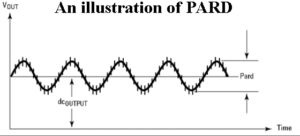
 PARD—Periodic and random deviation is the deviation of the dc output from its average value with all other parameters constant. It is a measure of the undesirable ac and noise components that remain in the dc output after the regulation and filtering circuitry. It is measured in rms or peak-to-peak, the latter being more common; over a bandwidth range of 20 Hz to 20 MHz. PARD-like variations that arise below 20 Hz are usually called drift.
Load Response—This can refer to a static or transient load and is a measure of a supply’s ability to remain within specified output limits for a predetermined load. Load response usually includes a measurement of the transient recovery time of the supply. This is the time needed to settle within a predefined band in response to a load change.
Noise—This is a deviation of the dc supply from its nominal value. Noise can include random noise, like thermal noise, and spurious signals such as switching waveforms coupling in from adjacent circuits or PARD and load response.
PDN Impedance— This is the impedance-versus-frequency of the PDN, with or without the dc/dc converter. Often a target impedance is determined during the design phase based on acceptable voltage variation, and then it is measured on the
actual target.
The idea of analyzing the power distribution path is not novel. Engineers have been working with the concept of measuring voltages and currents on power lines since the 1920s. What, then, has led to the current urgency to make PI measurements?
As IC gate density rises, so does the power density of ICs. More gates in a smaller space result in more current consumed in that same small space. Even if the current draw of each gate is reduced, the higher number of gates in that small area offsets the savings. Power, being the product of voltage and current, will therefore rise. This higher power consumption can lead to thermal failures, reduced battery life, a larger environmental footprint, and higher product costs from bigger/more power supplies, more cooling fans, more heat sinks, and larger enclosures.
To reduce power demands, designers have dropped operating voltages. As silicon geometries have shrunk, IC operating voltages have dropped as well to prevent their damage. Core voltages for microcontrollers, FPGAs, and memory ranged from 3.3 to 5 V twenty years ago and have steadily declined. Modern microcontrollers and FPGAs have a Vcore of 0.9 to 1.3 V while some LPDDR4 memories have a 0.6-V supply.

Simply reducing dc voltages is not enough. Previous-generation products with 5-V supplies commonly had a tolerance of ±250 to 500 mV. That same leeway on a modern microcontroller or FPGA would equate to ±25 to 50% tolerance on a 1-V supply leaving such a device inoperable. Supply tolerances have shrunk along with operating voltages and today they are typically 1 to 3% (±10 to 30 mV for a 1-V Vcore). These tolerances include the dc level and static and dynamic transient current response of the supply. As the amount of acceptable dc supply variation has shrunk, it has become increasingly important to verify the PDN performs as needed to prevent product failures.
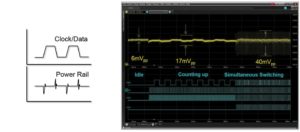
Transient current loads challenge the dc supply to maintain voltages within the specified limits, from dc up to the bandwidth of the switching current, typically above 1 GHz. The classic example of a transient current load is that of a digital line and its associate switching load on the supply. As the digital line goes from low to high it creates a sudden current load that may result in a temporary dip in supply voltage. When the same line goes from high to low it releases the load on the supply that potentially results in a momentary spike on the supply.

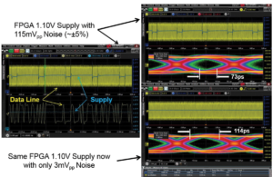
What happens if dc is not in spec? A loss or compromise of functions is at stake if the dc supply variation is not controlled. Excessive noise on the power bus may degrade operation and cause data corruption. Device delay is affected by variations in the dc supplying that device. As the supply voltage drops there’s more delay through the gates of that device and vice versa. Thus, variations in supply voltage translate into timing jitter, referred to as power supply induced jitter (PSIJ). Power supply noise is one of the major sources of timing jitter. For example, it is possible to see up to a 50% wider eye diagram on signals from FPGAs if core voltage variations are reduced from 5% to below 1%.
The need for PI is compounded by the growing number of dc supplies inside products today that must be measured and verified. Solid-state drives typically have 12 or more dc supplies while entry level tablets have about 24 dc supplies. Modern test equipment like oscilloscopes have about 75 dc supplies, and next-generation mobile products are approaching 200 supplies.
There are usually only a handful of unique dc voltages inside a product. The supply count rises because many products carry multiple copies of common dc supply voltages. There may be several different functional blocks inside a product that operate from the same voltages, but each block is given its own supply to prevent interaction or supply contamination from the dynamic loads constituted by the other functional blocks.
For example, when a Bluetooth module begins to transmit data it will present a sudden load on the supply because of inrush current. If another resource shares that supply, the compounded supply load may degrade its operation. To avoid the problem, it is common to arrange things so subcircuits have their own dc/dc converters acting as a buffer to prevent the loading of other subcircuits.
In all, modern life is filled with electronic products which all depend on the prosaic dc supply to function properly. Engineers and technicians responsible for bringing these products to market must ensure these products have dc supplies that meet specifications under all operating conditions.
REFERENCES
KEYSIGHT TECHNOLOGIES
BOGATIN, E. SIGNAL AND POWER INTEGRITY—SIMPLIFIED, 2ND ED., PRENTICE HALL, 2010.


Leave a Reply