Since the first application of the wheel, an element of all practical engineering projects has been the make-or-buy decision. The issue is fractal, arising at every level of the design hierarchy: For any given function, at some level of abstraction, you’ll choose to switch between make and buy. But the decision doesn’t hinge on a particular degree of design complexity or level of granularity that’s consistent across an entire system. Concepts like key value-add, core competency, opportunity cost, design risk, and sustainable competitive advantage mix with more concrete and measurable notions of time-to-market; BOM (bill-of-materials), inventory, assembly, and sustaining costs; and how to allocate engineering resources.
Even the common POL (point-of-load) converter — potentially exploited by the dozen in handheld devices and by the hundred in rack-sized systems and larger — raises a make/buy question. In the case of the POL, the question most often boils down to the level of power-train integration you choose for each instance of the function. Even within a single system design, the answer may not always be the same as some combinations of load voltage, load current, regulation tolerance, transient response, and power density pose greater engineering challenges than do others.
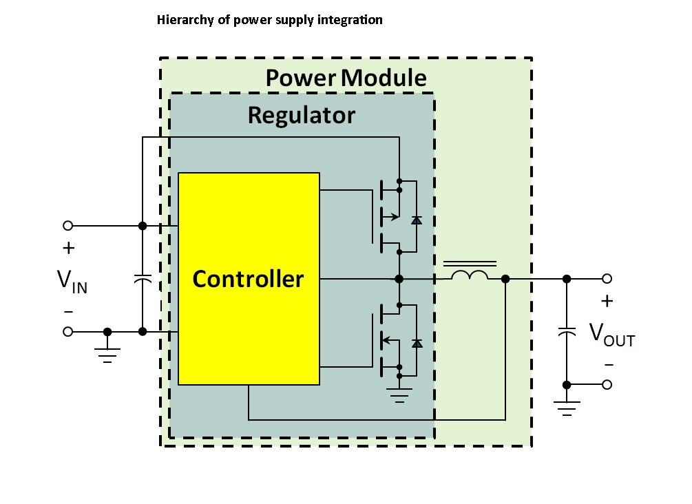 There are generally three levels of power-train integration to choose from for POL applications: The controller, the regulator, and the power module. Schematically, these look so similar as to hardly be worth discussion. The differences in their design-in and ongoing sustaining-engineering loads, however, are significant and well worth consideration.
The converter block typically comprises a voltage reference, oscillator, pulse-width modulator, dual-phase gate drivers, and either a hardware or hardware/firmware implementation of one of several feedback-based control methods. The regulator integrates the power MOSFETs and the power module brings the inductor into the package as well, requiring only input and output capacitors.
So-called discrete designs, based on a controller and separate MOSFETs and inductor, remain the least expensive in terms of BOM cost. They are also the most flexible in terms of the thermal and mechanical aspects of the design. For example, discrete power MOSFETs are available in a variety of current capacities and packaging options with various footprints, board heights, and thermal qualities. These let you select a power MOSFET package that is most compatible with the rest of your mechanical and thermal design. Additionally, discrete designs keep much of the losses and, thus, the power train’s heat generation out of the controller package, potentially improving overall performance over temperature.
As semiconductor technologies have advanced, switching frequencies have risen from the tens of kilohertz common at the advent of SMPSs (switched-mode power supplies) to well over 1 MHz for the fastest modern controllers. As switching frequencies have risen, power train sensitivities to layout parasitics have as well. For example, gate drivers have higher output impedances than do the power MOSFETs. Waveform-edge fidelity at the gate drive is critical so while discrete designs do offer a modicum of flexibility, it is just that: Even small stray inductances in the gate drive paths can degrade power-stage performance, so short and wide traces are always in fashion for these lines.
Additionally, RFI emissions are a function of the surface area described by the high-frequency current loops. Here again, tight layouts provide best results. Reference layouts from converter manufacturers serve as excellent guidance, and departures deserve engineering attention with this performance attribute in mind.
Further integration of the power train complicates the thermal design for regulators and power modules. Each successive level of integration benefits from significant vendor engineering effort to optimize the internal layout, minimize RFI emissions, develop reliable thermal models, and generate dependable application guidance to simplify system designers’ tasks.
The substantial growth in system complexity results in ever-lengthening feature sets, higher signaling bandwidths, faster information-processing speeds. These more complicated systems also need more sophisticated power management. Tight supply tolerances, the need to facilitate load shedding, and the need to prevent supply-coupled load-to-load interactions have all contributed to the burgeoning number of POL (point-of-load) power converters in modern system designs.
The trend toward higher converter switching frequencies has helped constrain the quanta of energy a power train processes per cycle and, correspondingly, reduced the size of reactive components needed to support a given output current. Along with high-speed control loops, this trend has also greatly improved typical load-current transient-response characteristics.
But the same trajectory has driven power management to take on some of the same attributes as high-speed signal processing systems as found in communication and computing applications. Signal integrity concerns are high on the list of issues challenging PCB layout designs and interface-circuit performance but with one important distinction: High-speed signal transmission and processing interfaces tolerate a certain degree of ISI (inter-signal interference). Indeed, this tolerance, in both timing and amplitude, is a fundamental advantage of digital signals.
By contrast, gate-drive signal fidelity for a power stage is critical and even small errors of gate-signal edge timing, rise time, or fall time can degrade performance. This is particularly true now that energy efficiency expectations for power stages often exceed 95%. In these cases, edge fidelity may be observed on a time scale of single-digit nanoseconds or even a few hundred picoseconds.
Here, power MOSFET selection is far more complicated than simply finding a suitable RDS(on) (channel resistance) and VTH (threshold voltage). And there’s more to designing the circuit than just matching a driver’s dynamic signal capability with MOSFET gate capacitances and connecting the two through an ultra-low inductance copper feed. So it comes as no surprise that higher levels of regulator integration have become more widely used.
 Looking at the choice from the perspective of how to segment things, the regulator is a more natural arrangement than the controller: The gate drives have higher impedance feeds and are extremely sensitive to board strays and interfering signals. The regulator output offers a lower source impedance and is far more robust in the face of layout strays. For example, a series stray inductance is of little consequence, given that the regulator output goes directly to an explicit inductor—the input to the two-pole LC filter. If anything, the series stray resistance that inevitably accompanies an inductive layout stray is the bigger concern because it raises power dissipation in the power train.
The third and highest level of power-train integration for POLs is the module. It brings the inductor into the package, forming a complete functional block that requires only bypass capacitors on the input and output.
Like the inclusion of the power MOSFETs when moving from the controller to regulator, the inclusion of the inductor in the shift from regulator to module looks, at first glance, like a minor value-add that slightly boosts BOM cost. The inclusion of the inductor, however, is helpful to module users and is increasingly compelling as requirements for output current and power-density grow.
This higher level of integration lets the module vendor more precisely characterize and specify the power converter end-to-end performance as presented in the application. As when combining the controller with power MOSFETs, combining these important power-train components in the module package protects against supply-chain interruptions and unauthorized component substitutions at a contract assembler. (I know, your contract assembler has never done anything remotely like that.)
Like most components, there’s more to an inductor than its inductance. With efficiency expectations often exceeding 95%, the inductor ESR (equivalent series resistance)—one of the inductor’s dissipative parasitics—is a strong inverse function of the winding wire gauge: ESR is proportional to the inverse square of wire diameter. Size and cost, of course, vary with wire size. Additionally, now that many power trains operate at near-RF frequencies, the skin effect increases the inductor resistance—and, correspondingly, resistive dissipation—for the converter’s harmonic current. A second dissipative term is the core loss and, here again, strict source quality control is a must for consistent field performance.
Another benefit of bringing the inductor into the power-converter module package is, ironically, thermal management. The primary dissipative elements in a power converter are the power MOSFETs and inductor, so bringing them inside the package might not seem to be the best way to simplify the thermal management. Yet it can be:
Power-regulator and -module vendors invest substantial engineering resources into developing and modeling thermally-efficient packaging technologies. This is an important and oft-underappreciated part of module value proposition in two areas: First, you get to buy a completely characterized block for which all of the dissipative elements have been factored in. So your design confidence is greater than with less-integrated implementations. Second, module packages provide a unified height for the entire converter, which reduces the system-level thermal-interface complexity and, thus, the thermo-mechanical design-in cost for the power train.


Leave a Reply