
Analog-to-digital converters (ADCs) need a reference voltage (VREF) input in order to operate properly. ADCs convert analog inputs that can vary from zero volts on up to a maximum voltage level that is called the reference voltage. The reference voltage determines the ceiling of what the ADC can convert, and is essentially the yardstick against which every proportion and result is measured. Therefore, in choosing a reference voltage (VREF) the voltage output level and initial accuracy are of the first concern.
VREF is also related to the resolution of the ADC. The resolution of an ADC is defined by dividing VREF by the total number of possible conversion values. (Think of the resolution of the ADC as equivalent to the smallest step size of the ADC.)
Attributes like precision, accuracy, and low noise are important for the ADC’s voltage reference, and the type of device used to provide the reference voltage for a data converter matters. The voltage reference is external to the ADC, and along with an amplifier to drive the reference, contributes to the overall system noise.
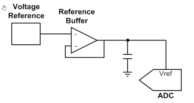
For microcontrollers (MCUs) that have integrated (internal) ADCs, you may or may not have control over the reference voltage. Some MCUs have an external pin that allows you to provide a voltage reference of your choosing, but others will simply use the MCU’s supply voltage. This can cause inaccuracy, for example, if the MCU accepts 3.3 V analog inputs to the internal ADC while the VREF for that internal ADC is actually the supply voltage to the MCU or 5V. In the end, the power supply, which can reasonably vary by as much as 3%, can cause a fairly significant change to conversion results.
As mentioned in a previous article on ADCs, a 10-bit ADC has 210=1,024 possible steps. The value produced by a 10-bit ADC with a 5V reference and a 3.3V analog input signal (where 3.3V is the highest value measured at the input) would be:
(VIN x 1,024) /VREF = (3.3 V x 1,024)/5 V = 675.84
However, the result, if V REF were 3.3 V, rather than 5 V, would be:
(VIN x 1,024) /VREF = (3.3 V x 1,024)/3.3 V= 1,024
On the other hand, if the power supply or voltage device that is used for VREF varies, the results can differ, even if the same analog input of 1.65 V is received by the ADC:
at VREF = 3.5 V: (VIN x 1,024) /VREF = (1.65 V x 1,024)/3.5 V= 482.7
at VREF = 3.0 V: (VIN x 1,024) /VREF = (1.65 V x 1,024)/3.0 V= 563.2
The variability of the voltage supplied to VREF is a large factor in the accuracy of your ADC. Power supplies or voltage regulator outputs can vary for several reasons that can be based on temperature and load fluctuations, and with variations from supply to supply, among other things.
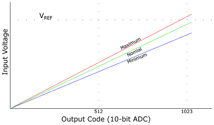
The VREF for your ADC should be very stable regardless of the temperature it experiences. It should demonstrate excellent performance over temperature. In short, the lower the number of ppm/°C, the better. Additionally, the initial output voltage accuracy of VREF should be low, in the range of 0.5% or less for precision ADC applications. The voltage reference should have noise value specifications lower than the ADC. The topology of the series voltage reference (as opposed to a shunt voltage reference) favors a better initial voltage performance and low drift over temperature.[i]
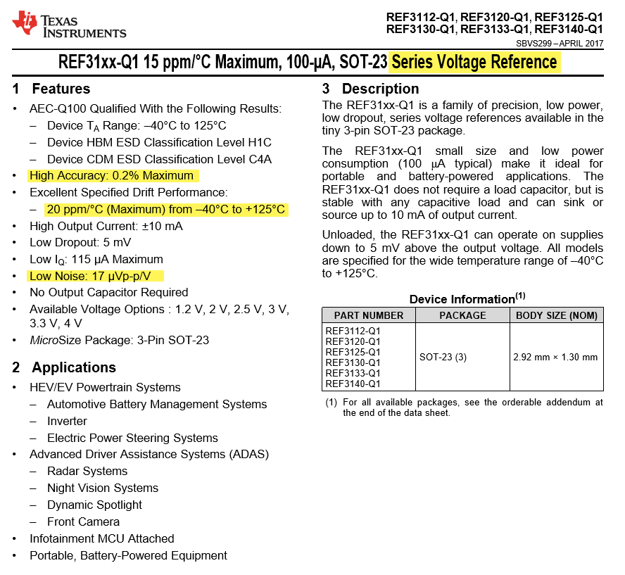
As an example, interpreting a datasheet for the TI REF31xx-Q1 series voltage reference shows high accuracy at 0.2% maximum, which means it will not vary more than 0.2% from the nominal value and an excellent specified drift performance over temperature of 20 ppm/°C (maximum) over operating temperatures from –40°C to +125°C. It’s also identified with low output noise at 17 µVpp/V. The other benefit is that the part comes in several voltage options offering VREF at 1.25 V, 2 V, 2.5 V, 3 V, 3.3 V, or 4 V.
The stability of the voltage provided as VREF over varying temperatures is very important. If not, then the ADC will give results that are skewed around the temperature at which it was first calibrated.
VREF should also be a value that is close to the maximum value that the analog input on the ADC will see. For instance, a signal at its highest value (pegged) at 3.3 V into the analog input to the ADC should relate back to a VREF of 3.3 V into the ADC. It is possible to compensate for variations in VREF using software and thereby calibrating the ADC, but this creates another potentially intensive task for the processor.
[i] Baker, B., & Oljaca, M. (2009, 3Q). How the voltage reference affects ADC performance, Part 2. Analog Applications Journal. Retrieved August 20, 2017, from http://www.ti.com/lit/an/slyt339/slyt339.pdf

Hello,
As mention in this article Vref value should be close to maximum ADC input voltage as much as possible.
i have to some query related to this.
in my project i want to make battery monitoring system using ADC pin with STM30F0 controller
i have to use 3.7 lipo battery. when battery is fully charge its voltage is 4.2 and when full discharge it is 3v.
i have to use voltage divider to divide voltage.
Maximum input voltage at ADC pin is 2.1 and minimum is 1.5.
i have to set my Vref 3.3v.
my question is : is this fine or i have to change my Vref to 2.1v
any problem is occur if i give 3.3v as reference voltage.
Thank you
nice article..
Vref Should Be > Or = Max Vin ,; Resolution (Proportional To) = Error ; Resolution (Proportional To) = Vref; So You Have To Low The Vref But It Must Not Be Less Than Vin At Any Instant Of Time ..So I Think If You Change Vref To 2.1V It Will Give Less Error ….
@Sashikant Prajapati ….
Indradeep Bhattacharyay
BTECH(WBUT)