Circuit designers increasingly must concentrate on the design of transmission lines, or the “spaces” between traces, instead of the “wires” on a circuit board.
By Daniel Beeker, Technical Director, Automotive Field Applications Engineering, Senior Member, IEEE, NXP Semiconductors
When it comes to the design of printed circuit boards, the industry focus has been on the movement of charges in the traces. The fact that design engineers don’t always appreciate is that current flows only because electric fields are moving. More to the point, the fields carry the energy, not the displacement current. My apologies to EM physicists for oversimplifying these concepts, but this approach will boost the chances of success for most designs.
Engineering teams worldwide face increasingly difficult challenges in designing electronic products and realizing good signal integrity and compliance. Today, it’s common to expect that a design will fail EMC testing not just once but three, four, maybe even five times. Each time the design is retested, there is little confidence in success.
This cycle is expensive in both the time for a redesign and the cost of urgently refabricating the new PCB and assembly. The numbers add up quickly. The expense and delay in product certification are seldom budgeted or scheduled and directly affect the bottom line and the customers waiting for the product. Instead of designing the next big thing, teams are trying to fix the current one. Billions of dollars are lost each year designing products that most likely won’t work.
What is wrong here? This “Billion-dollar mistake” is rooted in the misunderstanding of the nature of electromagnetic energy. One drawing is to blame: It depicts a simple on/off switch controlling a light bulb powered by a battery. The perspective from this simple drawing has set the tone and philosophy for PCB design (Figure 1).
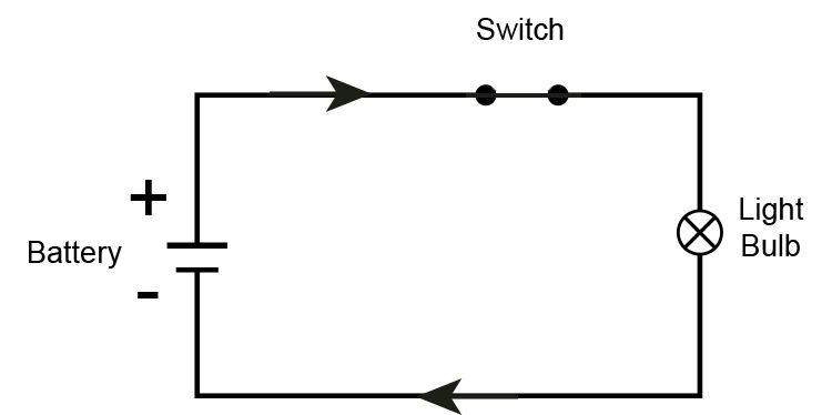
The focus has been on the current flowing in the conductor, and the result has been a steady rise in EMC failures as IC geometries grew smaller and switching frequencies rose. From this diagram, the wires started to be called “conductors” because the energy flowed in the wires. The current flowed in a loop, so the idea that this was a “circuit” was born.
But not so fast: If the energy was instantly seen at the load when the switch closed, there would be no signal integrity or EMC problems. There would also be no such thing as radio because the same energy in an electrical system is also in the air. Also, there would be no life on earth, as the light from the sun would not travel here without wires.
News flash: The wires are not conductors; they form boundaries, much like the banks of a stream. The energy does not flow through the wires; it travels in the space between them. This space, or dielectric, is the conductor. The energy is carried by the moving EM fields in the dielectric, not by electron flow in the wires. The current flow is the amount of EM field moving past a point in the transmission line.
Ralph Morrison — a pioneer in high-frequency/high-reliability electronic design — taught how important language is. In this case, incorrect language focusing on current in wires rather than fields sets the stage for bad design practices.
The norm became to design the conductors, connecting the battery or power source to the load. As long as the speed of the switch was relatively slow, this practice appeared to be the correct path. But as frequencies rose, the misconception led to design practices that almost guaranteed failure. The situation is analogous to the tale of the frog in the pan of water. The frog does not notice the water heating up until it is too late.
The reality
We are taught that electrical energy comprises electrons moving in the conductors. Switches add conductors, and the current instantly starts to move in the loop. The wires carry the energy, and the load instantly sees the energy flow. Wrong! Switches add new spaces, and the moving field carries the energy. It takes time for the field energy to move into that space. The moving field energy has no idea what is at the end of the new space. Current flow is the field energy moving through space.
Current (noun): a flowing; flow, as of a river; something that flows, as a stream, a large portion of air, a large body of water, etc., moving in a particular direction; the speed at which such flow moves; velocity of flow.
Notice that this definition (from dictionary.com) has nothing to do with the stream bed or the banks. The water flows in the space, not the land. The river’s current flow reflects the amount of water passing through, and the same is true for electromagnetic energy. Electrical current flow is a measure of moving EM fields in the space between the conductors that bound them.
The path to good design, when the focus is on the EM fields, is quite simple and can be summarized in three sets of three realities that Ralph Morrison called the rules of triplets:
1. You only need three components to contain EM energy: a space (dielectric) bounded by two conductors.
2. It takes just three components to build electronic systems: conductors, spaces (dielectric), and switches.
3. You can only do three things with electromagnetic field energy: Store it, move it, and convert it to kinetic energy (Figure 2).

EM field behavior on a PCB is equally simple to understand. The field goes where it is told. Managing the spaces is the key.
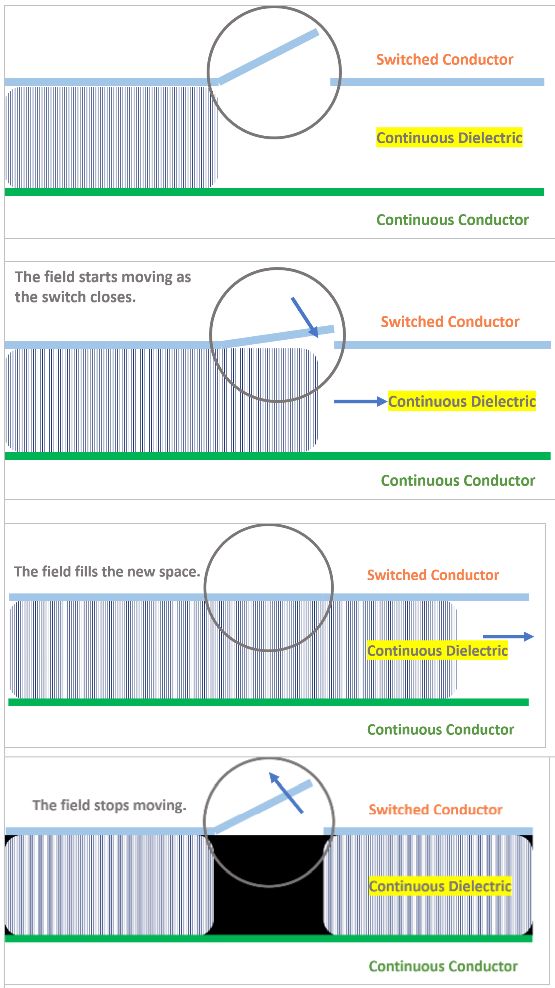
Consider the case of a switch closing on a PCB where the EM field is contained in a dielectric between a top and bottom conductor. When the switch is open, the field in the dielectric stops at the switch. The field starts moving beneath the switch in the dielectric as the switch closes and quickly fills the dielectric beneath the switch at switch closure. If the switch opens, the EM field stops moving and once again stops at the open switch.
Put simply, we are all just plumbers using leaky water pipes that happen to reside on a PCB. We design three-dimensional spaces for managing EM field movement (Figure 3).
Now consider power supplies. In a good design, energy is available whenever there is a demand, in the correct location, and connected with the appropriate plumbing. The impedance of the transmission line, not the resistance of the copper, is critical here. Adding heavier copper or more power vias is not the answer for higher current requirements. Matching the impedance to the demand is the key. Remember, the energy travels in the space. The solutions include wider power conductors, thinner dielectrics, or (my favorite) parallel dielectrics. You cannot get five gallons of water a minute through a one-gallon-a-minute hose by making it out of steel. The same goes for electromagnetic energy.
New problem: Moving this energy from storage to a load takes time. Wave velocity v for traces on a circuit board v = c/√ε, where c is the velocity of light and ε is the relative dielectric constant: v = 150 mm /nsec or 6 in/nsec. Electrons “drift” at the rate of 10-4 m/sec. They have mass, so they cannot approach the speed of light — more evidence that the fields, not the electrons, are doing the work. All energy is moved by wave action. When a switch closes, a voltage drop sends a wave to get more energy. Each reflected wave can carry a limited amount of energy.
The job of the PCB designer is to match the energy required for each type of switching event. As the geometry of the ICs we use continues to shrink, so does the area of effective power delivery. Well-defined power delivery transmission lines and small geometry, low-impedance field storage devices are essential.
Energy storage component geometry and placement requirements are determined by the device’s switching speed, not the clock frequency. The faster the switch, the more critical the geometry and placement. Do not expect behaviors from energy storage devices that are not possible due to their physical position or composition.
Critical factors include the distance from the switch, capacitor package size, and technology. The frequency at which capacitors can respond to energy requirements is determined by their physical geometry and the connecting transmission line, not by their value. Smaller capacitor packages respond faster because their terminals are closer together and provide more energy per wave cycle. Devices closer to the switch respond faster because it takes less time to request and deliver energy (Figure 4).
Oh, and by the way, energy delivery from power supplies is a one-way path! Current does not flow in a loop; it flows from the power source to the load. Each node in the power supply should be considered a discrete domain, with field energy traveling downstream from the power source to the switching device.
The key points to remember are:
Electromagnetic fields travel in the space between the conductors, not in the conductors.
Transistor switching speed determines the operation frequency, not the clock rate.
Switching speed determines the power supply requirements, not just the dc current specification.
Signal and power connections must be one dielectric from ground for their entire length (including layer transitions).
It’s All About the Space!
References
Ralph Morrison high-frequency design class,
“A novel approach to power distribution: Building a solid foundation,” notes,



Leave a Reply