• Skip to primary navigation
  • Skip to main content
  • Skip to primary sidebar
  • Skip to footer
  • Subscribe
  • Advertise

Power Electronic Tips

Power Electronic News, Editorial, Video and Resources

  • Products
    • Power Supplies
    • AC-DC
    • DC-DC
    • Battery Management
    • Capacitors
    • Magnetics
    • MOSFETS
    • Power Management
    • RF Power
    • Resistors
    • Transformers
    • Transistors
  • Applications
    • 5G
    • AI
    • Automotive
    • EV Engineering
    • LED Lighting
    • Industrial
    • IoT
    • Wireless
  • Learn
    • eBooks / Tech Tips
    • EE Training Days
    • FAQ
    • Learning Center
    • Tech Toolboxes
    • Webinars & Digital Events
  • Resources
    • Design Guide Library
    • Digital Issues
    • Engineering Diversity & Inclusion
    • LEAP Awards
    • Podcasts
    • White Papers
  • Video
    • EE Videos & Interviews
    • Teardown Videos
  • EE Forums
    • EDABoard.com
    • Electro-Tech-Online.com
  • Engineeering Training Days
  • Newsetter Subscription

Deep-depletion technique could bring better power MOSFETs

October 27, 2017 By Lee Teschler Leave a Comment

Researcher say the deep-depletion regime of bulk-boron-doped wide band gap semiconductors could be an avenue toward power MOSFETs able to handle large voltages and high temperatures.

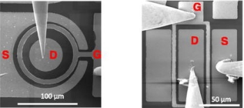
A group with members based in France, the UK and Japan applied the technique to diamond-based MOSFETs. But they say a similar scheme would work in other wide-band-gap semiconductors. They have used the idea to produce simple diamond MOSFET structures from single boron-doped epilayer stacks. This new method boosts a diamond-based MOSFET’s hole channel carrier mobility by an order of magnitude.

The group apparently thinks their approach is promising enough to commercialize. They have formed a start-up called DiamFab to bring the idea to market.

deep depletion
The three different conduction regimes: flatband regime, deep depletion regime, and inversion regime.
In a typical MOSFET, an oxide layer and a metal gate sit on top of a semiconductor material. Applying a voltage to the metal gate modulates the carrier density, and thus the conductivity, of the channel region under the gate. In the past, it has been tough to get enough charge carriers into the channel. The on-state current of a MOSFET strongly depends on the channel mobility which is often sensitive to roughness and defect states at the oxide-diamond interface where unwanted carrier scattering arises.

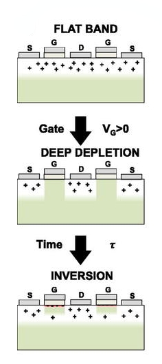
The deep-depletion concept is said to overcome the carrier scattering problem. To build their MOSFET, the researchers deposited a layer of aluminum oxide (Al2O3) at 380°C over an oxygen-terminated thick diamond epitaxial layer. They created holes in the diamond layer by incorporating boron atoms. Boron has one less valence electron than carbon, so its presence leaves a missing electron which acts like the addition of a positive charge, or hole. The resulting layer of material functioned as a thick conducting hole channel.

SEM deep depletion
SEM images of the diamond-based MOSFETs.
Applying a voltage switches the resulting transistor from on to off because the voltage repels and deplets the holes to form the deep depletion region. The idea won’t work in silicon-based transistors because this voltage would form an inversion layer and the transistor would not have turned off. The group says the special properties of diamond, and in particular its large band gap, suppressed formation of the inversion layer and made operation in the deep depletion regime possible.

The group described their work in Applied Physics Letters.

Filed Under: Power Components, Transistors

Reader Interactions

Leave a Reply

You must be logged in to post a comment.

This site uses Akismet to reduce spam. Learn how your comment data is processed.

Primary Sidebar

Featured Contributions

Ionic cooling: a silent revolution in thermal management

Robust design for Variable Frequency Drives and starters

Meeting demand for hidden wearables via Schottky rectifiers

The case for vehicle 48 V power systems

GaN reliability milestones break through the silicon ceiling

More Featured Contributions

EE LEARNING CENTER

EE Learning Center

EE TECH TOOLBOX

“ee
Tech Toolbox: Power Efficiency
Discover proven strategies for power conversion, wide bandgap devices, and motor control — balancing performance, cost, and sustainability across industrial, automotive, and IoT systems.

EE ENGINEERING TRAINING DAYS

engineering
“power
EXPAND YOUR KNOWLEDGE AND STAY CONNECTED
Get the latest info on technologies, tools and strategies for EE professionals.
“bills

RSS Current EDABoard.com discussions

RSS Current Electro-Tech-Online.com Discussions

  • Very low RF-DC conversion efficiency in ADS (SMS7630 & HSMS-282E)
  • Panasonic RQ-A170 Walkman recorder
  • Looking for obsolete item from Parallax
  • Can a small solar panel safely trickle-charge old NiMH AA batteries?
  • TraxMaker Pro? I only have the non-Pro version. Looking for the Pro version that has the integrated pick and place coordinates export.

Footer

EE World Online Network

  • 5G Technology World
  • EE World Online
  • Engineers Garage
  • Analog IC Tips
  • Battery Power Tips
  • Connector Tips
  • EDA Board Forums
  • Electro Tech Online Forums
  • EV Engineering
  • Microcontroller Tips
  • Sensor Tips
  • Test and Measurement Tips

Power Electronic Tips

  • Subscribe to our newsletter
  • Advertise with us
  • Contact us
  • About us

Copyright © 2025 · WTWH Media LLC and its licensors. All rights reserved.
The material on this site may not be reproduced, distributed, transmitted, cached or otherwise used, except with the prior written permission of WTWH Media.

Privacy Policy