Use of a negative gate drive can lead to a larger voltage drop during deadtime and severe losses.
Andrea Gorgerino, EPC
GaN devices have gone from initial R&D to mainstream designs over the last 15 years. Unfortunately, there are many misunderstandings left-over from those early-stage 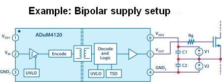 developments or dead-end technology branches. One of the most pernicious is the topic of bipolar drive. In actuality, unipolar drives are the best way to drive eGaN FETs.
Bipolar gate drives are still used in power electronic circuits. But their applications are usually confined to high-voltage-class devices (≥ 1,200 V) and high-current circuits where layout limitations and component parameters create concerns for the cross-conduction effect called Miller effect.
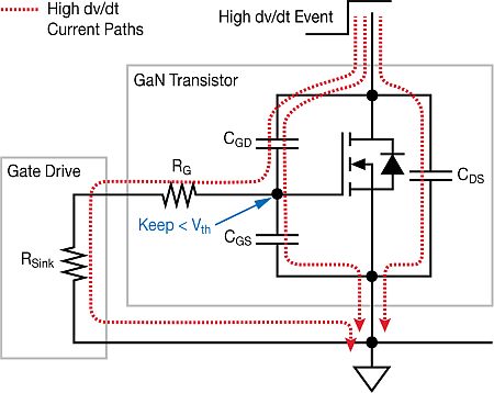
The Miller effect appears in half-bridge topologies and happens when the complementary device (which is OFF) is subject to a high dV/dt generated by the device in the other half of the bridge turning ON. During this event, the capacitors of the OFF device are charged by the external dV/dt.
The current of interest charges the gate-drain capacitance, also known as Miller capacitance: This current then flows either through the gate resistor and then the gate driver (which attempts to keep the device OFF), or through the gate-source capacitance. In turn, the current flowing through gate-source capacitance will create a voltage from gate to source. If this voltage exceeds the device threshold voltage, the device begins to conduct some current. This current is a shoot-through current because it comes from the main bus capacitor and flows through both half-bridge devices. This shoot-through current leads to additional switching losses and could even lead to device failure if the voltage on the gate, and hence the current, is high enough.
Several strategies have been implemented in MOSFET designs to mitigate this effect at the circuit design level. In increasing order of complexity they are:
Minimizing gate loop parasitics in the layout allows the gate driver to bypass part of the current coming through the gate-drain capacitance.
Use of separate turn ON and OFF gate resistors allows the design to reduce the dV/dt while maintaining a strong gate driver to keep the OFF device OFF. This method is most effective when combined with item one above
Finally, a driver with an active Miller clamp can be utilized. This concept can be considered an expansion of item two above, where an additional turn-OFF pin is available on the driver. This additional OFF clamp is active after the turn-OFF event and further helps to clamp the gate during dV/dt events. But the driver must have the clamp built in.
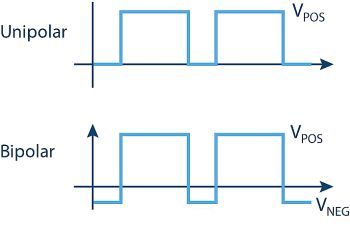
It is possible to drive the gate to a negative voltage using a bipolar gate drive. In this way the current flowing through the gate-source capacitance now must charge the gate from a negative voltage, e.g. -5 V, instead of from 0 V. This approach provides additional headroom before the threshold voltage is reached. But the technique requires generating two separate voltages for each device, so it can add significant cost and complexity to the overall design.
The Miller charge ratio
Circuit-level mitigation strategies for the Miller shoot-through can add complexity and cost. Before committing to any such strategies, it is important to look at the impact of the device itself and its characteristics on this effect.
The most important parameter to consider is the Miller ratio which is defined as either a ratio of capacitances or a ratio of charges. Because semiconductor devices have quite non-linear capacitances versus voltage, we will use the Miller charge ratio which is more accurate. It is defined as QGD/QG(TH), where QG(TH) is the pre-threshold voltage gate charge. This criterion also automatically takes into consideration the effect of different threshold voltages, as lower thresholds imply lower QGS(TH).
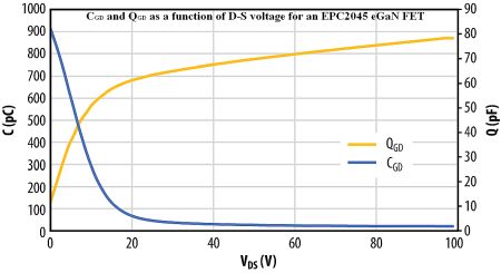
It should be noted that in most datasheets QGD is given at 50% of the maximum VDS of the device, while it is common to use FETs up to 80% of their rating. As an example, for an EPC2045 eGaN FET the difference in QGD from 50% to 80% voltage is about 10%.
Keeping the ratio as low as possible will minimize the voltage on the gate. More importantly, keeping the  ratio below one will ensure the voltage on the gate will always stay below turn-on threshold. If this criterion can be met, we are guaranteed to avoid any shoot through.
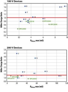
Miller charge ratios for EPC eGaN FETs are all below one. This means eGaN FETs are not susceptible to Miller shoot through! For comparison, many 100-V and 200-V-class silicon MOSFETs are quite susceptible to Miller shoot-through and care should be taken when using such devices.
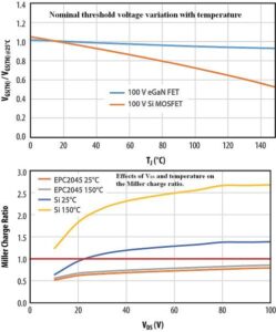
Another important consideration is threshold voltage variation with temperature. In silicon MOSFETs the threshold voltage falls with temperature. So when the device is at its operating temperature the QG(TH) can be as much as 50% lower than the datasheet value, which means a x2 factor on the Miller charge ratio. On the other hand, the variation for any eGaN FET is less than 10%.
By combining these two effects (gate-drain capacitance variation with voltage and threshold voltage variation with temperature) we can also see eGaN FETs are more stable than silicon MOSFETs regardless of Miller charge ratio calculated in nominal conditions.
In a nutshell, eGaN FETs don’t need bipolar drives. More specifically, bipolar drives should not be used because of reverse direction conduction in GaN FETs.
In a silicon MOSFET, a p-n junction forms a diode from the source to the drain of the transistor. Current flowing in the reverse direction (into the source) flows through this diode. This diode has the usual characteristics of a p-n diode such as a knee voltage around 0.7 V, and forward and reverse recovery.
In contrast, a GaN FET has no such diode. This quality is an advantage because it means QRR is zero. However, GaN FETs do conduct current in the reverse direction in a way like a diode. This reverse conduction path is formed by turning on the 2DEG in the reverse direction, using the positive gate‐drain voltage to enhance the channel. Therefore, if the gate voltage drops below 0 V, the reverse conduction voltage will rise by the same amount. Thus it is important not to use negative gate drive as to not increase this voltage drop.

This effect is only present during the dead-time interval, as when the gate is turned ON the GaN FET will conduct current with the same on resistance as in the forward direction. Although deadtime can be reduced thanks to the fast-switching characteristics of GaN devices, the additional losses when using a negative gate drive can still add up and are best avoided.
To illustrate the more severe loss due to a negative gate drive, consider a simple synchronous buck converter during deadtime conduction. We ignore the impact of negative drive on turn-OFF losses. The main conditions for the converter are:
700 kHz switching frequency
48 to 12 V, 10-A output
12 nsec deadtime
Turn-OFF VGS = 0 V or -2 V

Results graphed in the nearby figure reveal the overall losses increase by 10% from 2.4 W to 2.6 W.
We have shown why the need for bipolar gate drive for GaN FET is truly a myth. Thanks to the low Miller charge ratios always below one, the induced shoot-through will not happen. And use of a negative gate drive can actually lead to more severe losses because of a larger voltage drop during deadtime.
At EPC, our reference designs and demo boards are designed with unipolar gate drive (0 V turn OFF), optimized layout, and if possible, separate RgON and RgOFF. With these simple guidelines we can realize robust high performance.
References
EPC
J. Strydom, D. Reusch, S. Colino and A. Nakata, “AN003: Using Enhancement Mode GaN-on-Si Power FETs,” EPC, 2017. [Online].
R. Schnell, Analog Devices, 2018. [Online].
A. Lidow, M. de Rooij, J. Strydom, D. Resuch and J. Glaser, GaN Transistors for Efficient Power Conversion, Wiley, 2020.





Leave a Reply