
by Steve Roberts, Recom
A quick review shows the sources of inefficiencies in both linear and switching power supplies.
Most engineers know that one reason switch-mode power supplies have become widely used is their high energy efficiency. But many engineers don’t know power supply technology well enough to explain the sources of switch-mode efficiency and inefficiency. So it is useful to review how ordinary linear supplies dissipate energy and why their energy efficiency is so low. It can also be helpful to understand where energy leaks out of switch-mode designs. Different components have different sources of energy loss. And different switch-mode designs lose energy in different ways
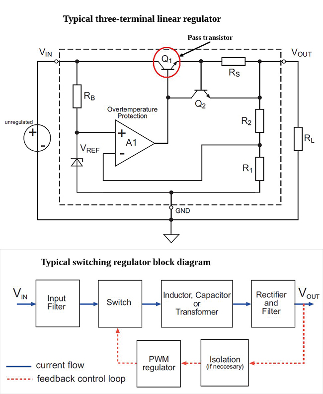
First, consider typical regulators for linear power supplies. They usually consist of a transistor in series between the input and output voltages. This pass transistor is the regulating element, effectively functioning as a variable resistor. It limits the current flowing from input to output. A resistor divider delivers a voltage at the input of an error amplifier equal to that of a reference voltage. The error amplifier produces an output driving the pass transistor. The action is such that the voltage difference between the inputs of the error amplifier is always zero. In other words, the error amplifier responds to changes such as a higher load or a rising or falling input voltage.
The efficiency, η, of a linear regulator is defined by the ratio of the delivered output power POUT to the power consumption PIN:
η = POUT/PIN
From Ohm’s law, Pout = Vout x Iout; Pin = Vin x Iin; Iin = Iout + IQ; where IQ is the quiescent current of the linear regulator when there is no load. The equation can be rewritten:
η = (VOUT IOUT)/VIN (IOUT+IQ)
Now consider an example of a typical 5-V, three-pin voltage regulator with an input voltage of 10 Vdc, output current of 1 A and a quiescent current of 5 mA. The efficiency calculation is then:
η = 5V x 1A/10V x 1.005A = 0.49
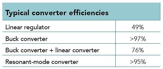
Thus, the overall efficiency is 49%. Note the power dissipation in the converter exceeds the 5 W delivered to the load. If the input voltage is lowered to the minimum of 7 Vdc, the efficiency rises to 70%, but this is the maximum practical efficiency as the regulator needs about 2 V of headroom for proper regulation.
It is immediately apparent from the efficiency equations that the efficiency of this type of regulator depends directly on the input voltage and load. And the energy efficiency is not constant. This also means the voltage regulator must be equipped with a heat sink large enough to allow safe operation under the worst-case conditions of maximum input voltage and maximum output current.
Now consider switching regulators. In contrast to linear regulators, which dump excess power as heat to limit the output voltage, switching regulators exploit the energy-storing properties of inductive and capacitive components to transfer power in discrete energy packets. The packets of energy are stored either in the magnetic field of an inductor or in the electric field of a capacitor. The switching controller ensures that only the energy actually required by the load is transferred in each packet. That’s why this topology is energy efficient.
The most common way to transfer the energy from input to output in a switching regulator is PWM (pulse width modulation), where a variable width pulse with a fixed time interval modulates the amount of energy transferred from input to output. The duty ratio of the PWM, δ, is the ratio of on-time ton (the time during which energy is drawn from the source) to the period T (the inverse of the switching frequency ƒOSC):
δ = tON/T where T = 1/ƒOSC
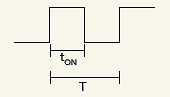
For many switching regulators, the regulated output voltage is directly proportional to the duty cycle of the PWM. The control loop uses the “large-signal” duty cycle to control the power switching element. In contrast, the linear regulator uses the “small-signal” servo loop to limit the current through the pass transistor.
One reason PWM control is much more efficient than linear control is because the main losses occur during each change-of-state of the switch rather than continuously. FETs that are full-on or full-off dissipate little power.
Compared to linear regulators, the process of determining the efficiency of switching regulators is much more complicated. The linear regulator has easily predetermined dc losses; the largest dissipation takes place in the pass transistor. A switching regulator, however, has not only dc losses but also ac losses that arise in the switches and in the components for energy storage.
For example, the total loss of a switch is made up of not just the loss in the on and off states, but also the losses in the transition from switching on and off. In the case of a transformer, the total loss is calculated from the sum of ac (core), ac (winding) and dc (winding) losses. The losses in the core of a transformer are caused mainly by the interaction between the magnetic flux and the core material (hysteresis losses, eddy current losses). The winding losses result mainly from the material of the transformer winding (ohmic losses, skin effects). Either way, the net effect is a rise of temperature in the transformer.
To calculate the efficiency of a dc/dc converter, the losses of each part of the conversion cycle must be found by averaging the losses over the whole range of the PWM duty cycle. The losses in the magnetic, inductive and capacitive components can be controlled and minimized to realize a high conversion efficiency. Typically only about 4% of the input power is lost and converted into heat.
Non-isolated converters are generally more efficient than their isolated counterparts because fewer parts are involved in the power conversion; non-isolated converters don’t use transformers, so there are no transformer losses. Yet despite a higher degree of complexity, isolated dc/dc converter efficiencies of more than 85% can be realized, depending on the power rating.
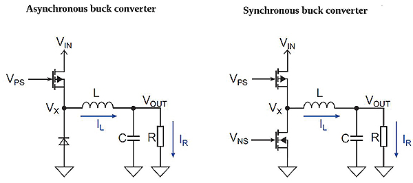
One of the major causes of efficiency loss in switch-mode circuits are the output diodes. If the output current is 1 A and the forward voltage drop across the diode is 0.6 V, then 600 mW will be lost in the diode alone. Thus, high output current dc/dc converters often use FETs with synchronous switching to reduce rectification losses.
It may be surprising to learn that lower-power converters generally have lower efficiencies than higher-power converters, especially considering the higher I²R losses that arise at higher output currents. However, the internal power consumption of the switching controllers, shunt regulators and optocouplers (the “housekeeping” consumption) plays a significant role. If the total housekeeping demand is 1 W, then a 10-W converter can not have an efficiency exceeding 90%. But the maximum possible efficiency of a 100-W converter would be 99%.
Housekeeping losses also explain why all dc/dc converters have 0% efficiency under no-load conditions, as the converters still consume power but deliver no output power. FETs consume more power when switching than in a steady on or off state. This is because their internal gate capacitance must be charged and discharged to switch the output. Peak gate currents of 2 A or more are not unusual. A dc/dc converter running with no load will still be switching the FETs hundreds of thousands of times per second, so it is not unusual for a dc/dc converter to still run warm without any load.
Factoring in parasitics
The level of energy efficiency among switch-mode converter topologies varies. One reason is that the components they use are non ideal. Textbook descriptions of converter topologies assume ideal components and ignore the parasitic effects. It is, however, a fact of life that inductors have capacitive and resistive elements and vice versa. The choices of components used in a switching supply therefore have a large influence on its performance. Critical components, such as switching and rectifying elements, magnetic components and filter capacitors, all affect both the switching frequency and also the overall efficiency of the converter.
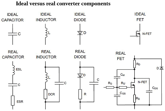
In particular, semiconductor switches have many non-ideal properties. FETs place high peak current demands on the driving circuit, especially the current needed to charge and discharge the parasitic Miller capacitance between gate and drain. Diodes have a parallel equivalent capacitance that slows their switching speed and, of course, the internal forward voltage drop. Inductor losses depend greatly on the choice of core material and have operational losses arising from I²R dissipation in the winding and coupling capacitances between the turns. Capacitors have parasitic effects such as equivalent series resistance (ESR) and equivalent series inductance (ESL). All these effects depend on frequency, so an inductor can behave as a capacitor at high frequencies, just as a capacitor can behave as an inductor.
Transformers have similar issues. The disadvantage of using a transformer is that the energy transfer from primary winding to secondary winding involves additional losses. So while a buck regulator can reach 97% conversion efficiency, transformer-based converters struggle to exceed 90%.
Parasitic elements
Parasitic effects in transformers include interwinding coupling capacitances for both the primary and secondary windings, a magnetizing inductance of the core, and leakage inductances for both the primary and secondary.
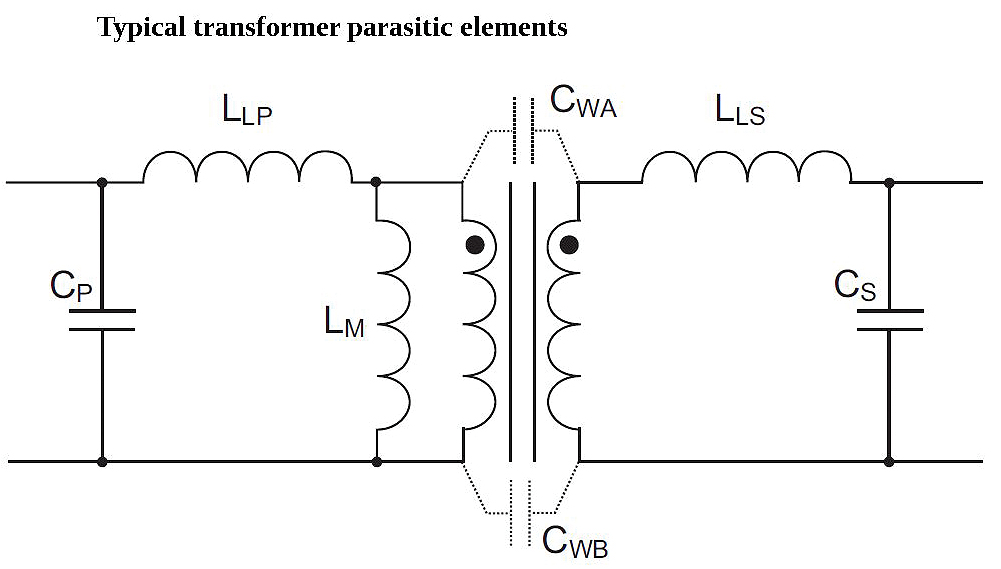
These transformer parasitic effects strongly influence the converter performance. Coupling capacitance causes common-mode EMC problems. Core saturation caused by magnetizing inductance limits the transformer current. Leakage inductances are especially troublesome, reducing efficiency and generating radiated EMI.
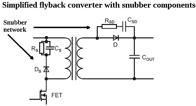
Leakage inductances are also responsible for the voltage spikes that arise whenever the current changes rapidly in the windings. Such overvoltages stress the primary switch and secondary diodes, so they must either be sized to withstand the peak voltage or fitted with a parallel snubber network to dissipate the energy in the spikes.
However, the energy in the spikes and the power that the snubber has to absorb constitute an energy loss that diminishes the efficiency of the converter. The energy in the spikes and the power that the snubber must absorb can be calculated according to:
E = 1/2 LLEAK I2LEAK
P = 1/2 LLEAK I2LEAK ƒ
A snubber cannot eliminate the power loss caused by the spikes. The power that would otherwise be dissipated in the switch or rectifier diode is now dissipated by snubber network resistors instead.
Besides the spikes caused by the parasitic leakage inductance, any coupled reactive system will also exhibit resonant frequencies. Most transformer-based designs try to either reduce these parasitic elements to a minimum or choose operating frequencies where resonance is not an issue. However, a quasi-resonant or resonant converter design deliberately encourages resonance by increasing the winding inductance or by adding additional inductors because controlling this resonance can facilitate an efficient converter design.
As has been mentioned before, one big source of efficiency loss in any converter is the power dissipation in the output diodes. Low forward-voltage-drop Schottky diodes can sometimes serve as an alternative for low-power converters, but they are expensive when sized to cope with higher currents. Even so, the forward drop is around 200 mV, so the power loss can still be significant.
A big leap forward in efficiency improvement has been the development of synchronous rectification.
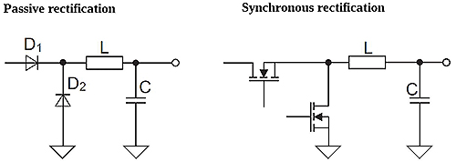
In a typical circuit with diode rectification, one diode acts as a rectifier and another is a freewheeling diode. Both diodes are alternately loaded with approximately the same current. The losses from the forward voltage drop in the diodes is just the voltage drop times the diode current. With a typical forward voltage of 0.5 V, a relative power dissipation of 0.5 W per amp can be assumed. A 3.3 V/10 A output converter would therefore have a voltage conversion loss of 15% without considering any other conversion losses. The power dissipated in the diode would be 5 W, so the diode would probably have to be heat-sink-mounted to have any useful operating temperature range.
Fortunately, FETs can be used as rectifying elements by switching them on during the forward part of the cycle and turning them off during the reverse part of the cycle. Their advantage as fast switches with low on-resistance makes them suitable as rectifiers.
The disadvantage of FETs is that they must be actively driven, so there are additional timing and drive circuits required. Synchronous rectifiers need to sense the internal voltages to correctly turn on and off the two FETs synchronously with the output waveform, hence the name of this topology.
In comparison, diodes are passive devices that need no extra circuitry to function, but the low on-resistance of FETs of about 10 mΩ more than offsets the disadvantage of the more complex circuitry for high output current converters.
Finally, a word about calculating efficiency: The efficiency of a voltage conversion is given by the ratio of output power to input power. At zero load, the efficiency is always zero. A specification in percent is common, but it can also be given as a normalized number (≤ 1). Normally, the data is provided under several conditions, such as nominal input voltage and full load.
References
Recom Electronic
recom-power.com
Leave a Reply