
By Durga Praveen G and Rakesh Panguloori, Texas Instruments
There is unprecedented demand for highly available and redundant systems to offer the best user experience. For example, in communications, banking, and industrial automated systems, any amount of system downtime could potentially lead to lost customers.
The implementation of a hot-swap circuit at the input of these systems protects against system faults and avoids system resets during power-supply disturbances. A hot-swap circuit comprises a hot-swap controller along with an external metal-oxide semiconductor field-effect transistor (MOSFET) and sense resistor in the power path, as shown in Figure 1. As the power level of the module increases, the circuit requires more MOSFETs in parallel for lower path resistance and better thermal management.
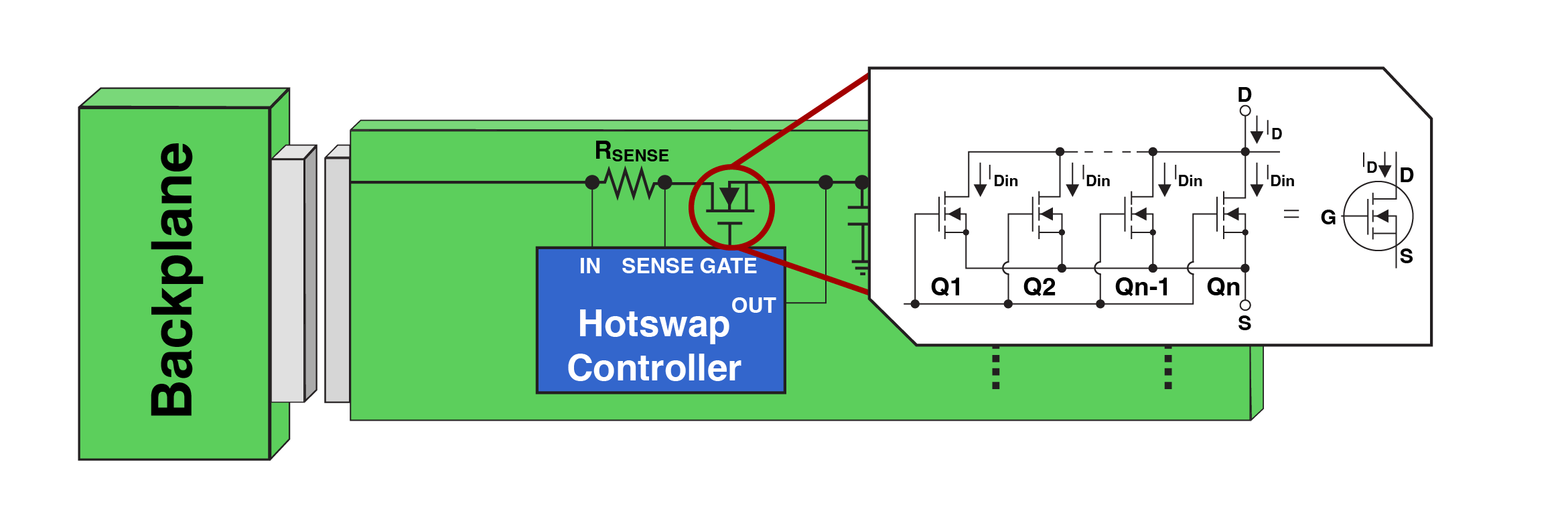
A hot-swap controller generally has the option to program the current limit threshold (ILIM), power limit threshold (PLIM) and timer duration. During fault scenarios, the hot-swap controller regulates the MOSFET’s gate, forcing the MOSFET to operate in the saturation region so as to limit the current flowing in the power path or power dissipation in the FET to their respective thresholds. If the fault condition persists, the MOSFET turns off after the timer expires; therefore, the MOSFET used in the design must have safe operating area (SOA) limits high enough to withstand power loss during the timer period. For a more detailed understanding of MOSFET stress in different fault scenarios, see the Texas Instruments application report, “Robust Hot Swap Design.”
Challenges in traditional hot-swap designs
The traditional hot-swap circuit design process is complicated, involving multiple parameters and complex calculations. Selecting a MOSFET with an appropriate SOA that can withstand power stress in various fault conditions is one of the most important steps in a hot-swap design implementation. Designers also need to consider system-level specifications such as the maximum input voltage (VIN(MAX)), maximum load current (ILOAD(MAX)), total output capacitance (COUT), duration of transient load, and the maximum ambient temperature (TAMB(MAX)), along with FET parameters such as SOA, the drain-to-source on-resistance (RDS(ON)) and the thermal resistance (RθJA).
At the start of the design process, you will not know which FET is right for your application. As you can see in Figure 2, the designer picks a FET based on VIN(MAX) and ILOAD(MAX) and goes through a series of complex design steps to find out whether the selected FET has an SOA strong enough to meet the application requirements.
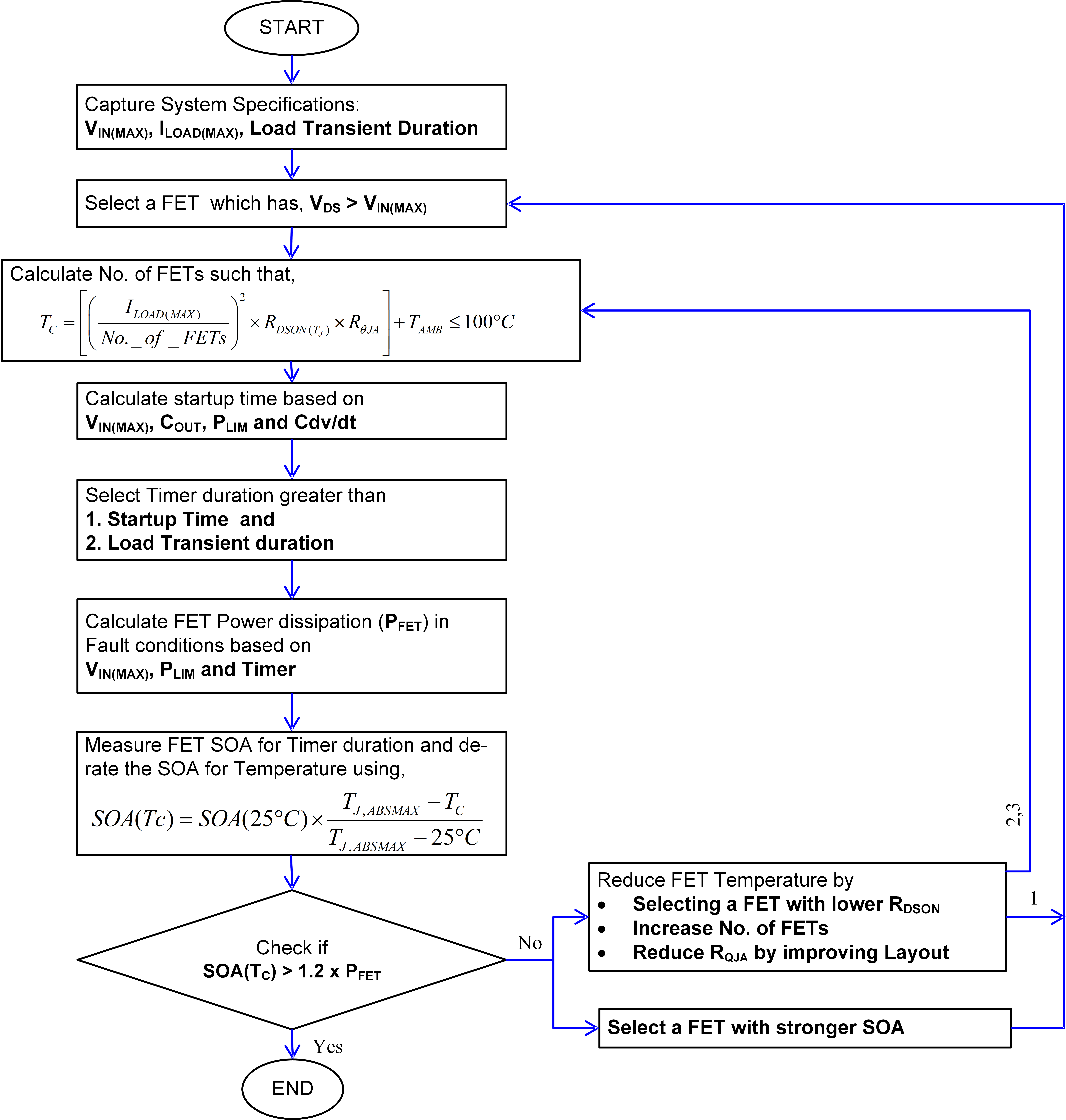
Here are the steps involved in the design flow:
- Calculate the number of MOSFETs required in parallel based on ILOAD(MAX), TAMB(MAX), FET RDS(ON) and RθJA.
- Calculate the time required for starting up into output capacitance. Designs with a large COUT require a transient voltage (dv/dt) control circuit with a capacitor (Cdv/dt) from gate to ground in order to limit the inrush current. Your startup time calculations should consider VIN(MAX), COUT, PLIM and Cdv/dt.
- Select a timer duration greater than the startup time and load transient duration.
- Calculate the energy dissipated in the FET based on VIN(MAX), PLIM and the timer in different conditions, especially startup into an output short-circuit fault. To simplify the analysis, assume that the calculated energy is a square pulse with time (for example, tx) and that the power is the peak power dissipated (PFET) during a fault condition.
- Estimate the amount of power stress that the MOSFET can handle for tx duration, as the FET data sheet may not provide the power-handling capability for the exact tx This step involves the proper extrapolation of data in the SOA graphs approximating that the FET power handling vs. time follows a line on the log-log plot.
- Derate the FET’s power-handling capacity for the maximum FET junction temperature based on ILOAD(MAX), TAMB(MAX), FET RDS(ON) and RθJA.
- Compare the power dissipated (PFET) in the FET during fault conditions to the derated power-handling capacity of the FET, checking whether there is at least a 20% SOA margin.
- If the margin is less than 20%, restart the design process after improving at least one of these parameters:
- Selecting a FET with a lower RDS(ON).
- Increasing the number of FETs in parallel.
- Reducing RθJA by improving the layout.
- Selecting a FET with a stronger SOA.
Every parameter change requires that the designer rerun the entire design flow and confirm whether the SOA margin is satisfactory. The entire design process is highly iterative and cumbersome until the designer finds a suitable FET. Texas instruments has design calculators for hot-swap controllers that can help when designing and reviewing the SOA margin for designs; however, engineers inexperienced in hot-swap circuit design may still find it difficult to select the most suitable FET.
Simplifying hot-swap design using a hybrid hot-swap circuit
A hybrid hot-swap circuit consists of an eFuse connected in parallel with a traditional hot-swap circuit, as shown in Figure 3. An eFuse is a hot-swap controller and MOSFET integrated into a single package, along with additional features such as thermal protection that protects the FET during power stress and ensures its operation within SOA limits. The power-good signal of the eFuse connects to the enable pin of the hot-swap controller, and the power-good signal of the hot-swap controller connects to the enable pin of the downstream load. These connections ensure that:
- The hot-swap FETs turn on only after the eFuse charges the large output capacitor close to the input voltage. The FETs start up with almost zero voltage across them, eliminating power stress during startup.
- The downstream load is enabled only after the hot-swap FETs are fully enhanced; the FETs can offer a low impedance path (compared to the eFuse) and share the majority of the load current.
- The eFuse endures power stress during all fault conditions, and the hot-swap FETs are not subjected to stress in any condition.
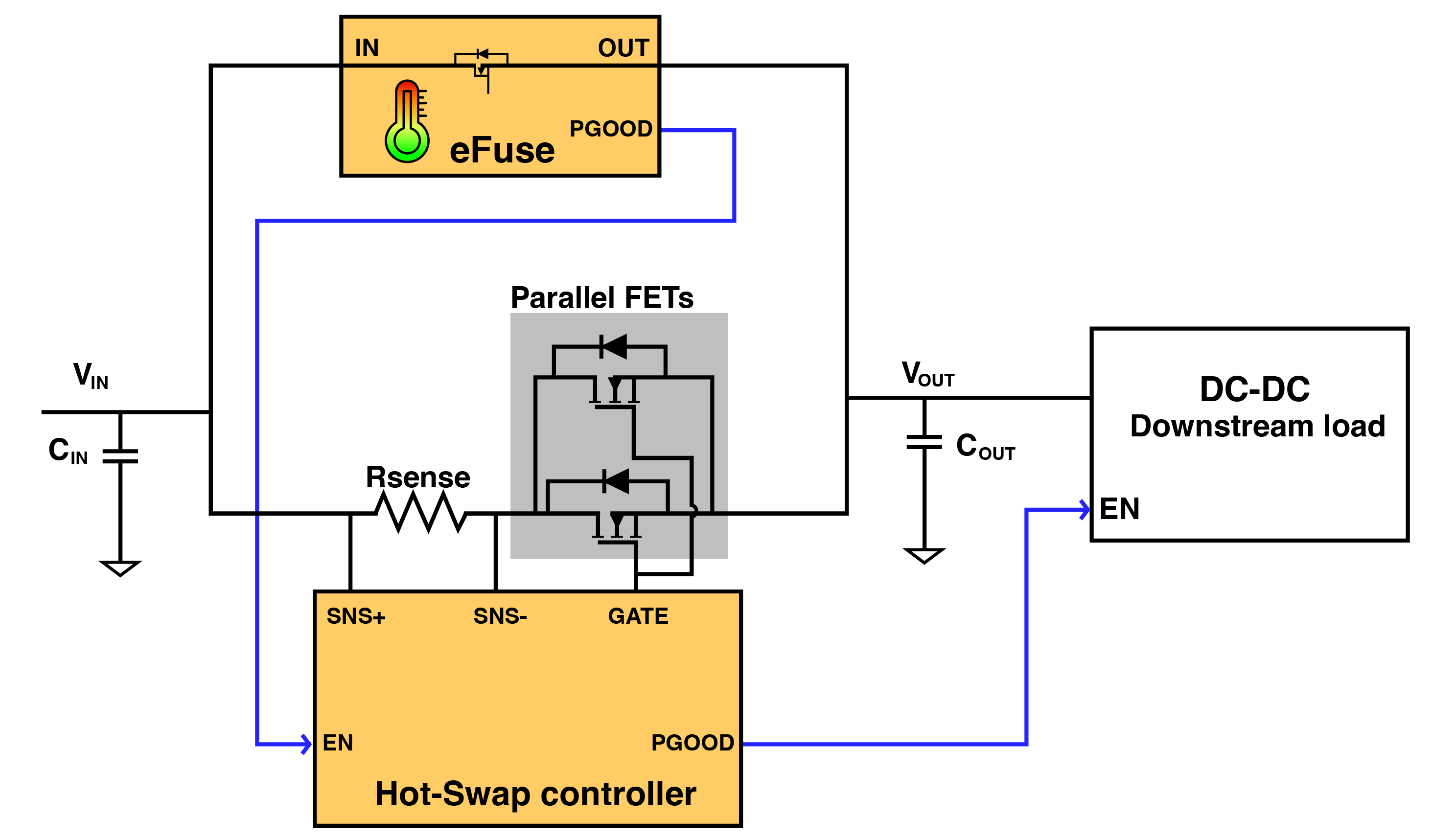
eFuses have an integrated overtemperature protection function that protects the internal FET by turning it off when the junction temperature reaches a certain threshold. eFuse devices such as the TPS1663 from Texas Instruments also have a thermal regulation loop that enables the maximum utilization of its internal FET power-handling capability during startup into capacitive loads and other fault conditions. Making use of this protection feature, the hybrid hot-swap circuit is designed in such a way that the eFuse is subjected to all stressful events. The hot-swap FETs are off during these conditions, thereby eliminating the most critical challenge in a traditional hot-swap design – the FET SOA.
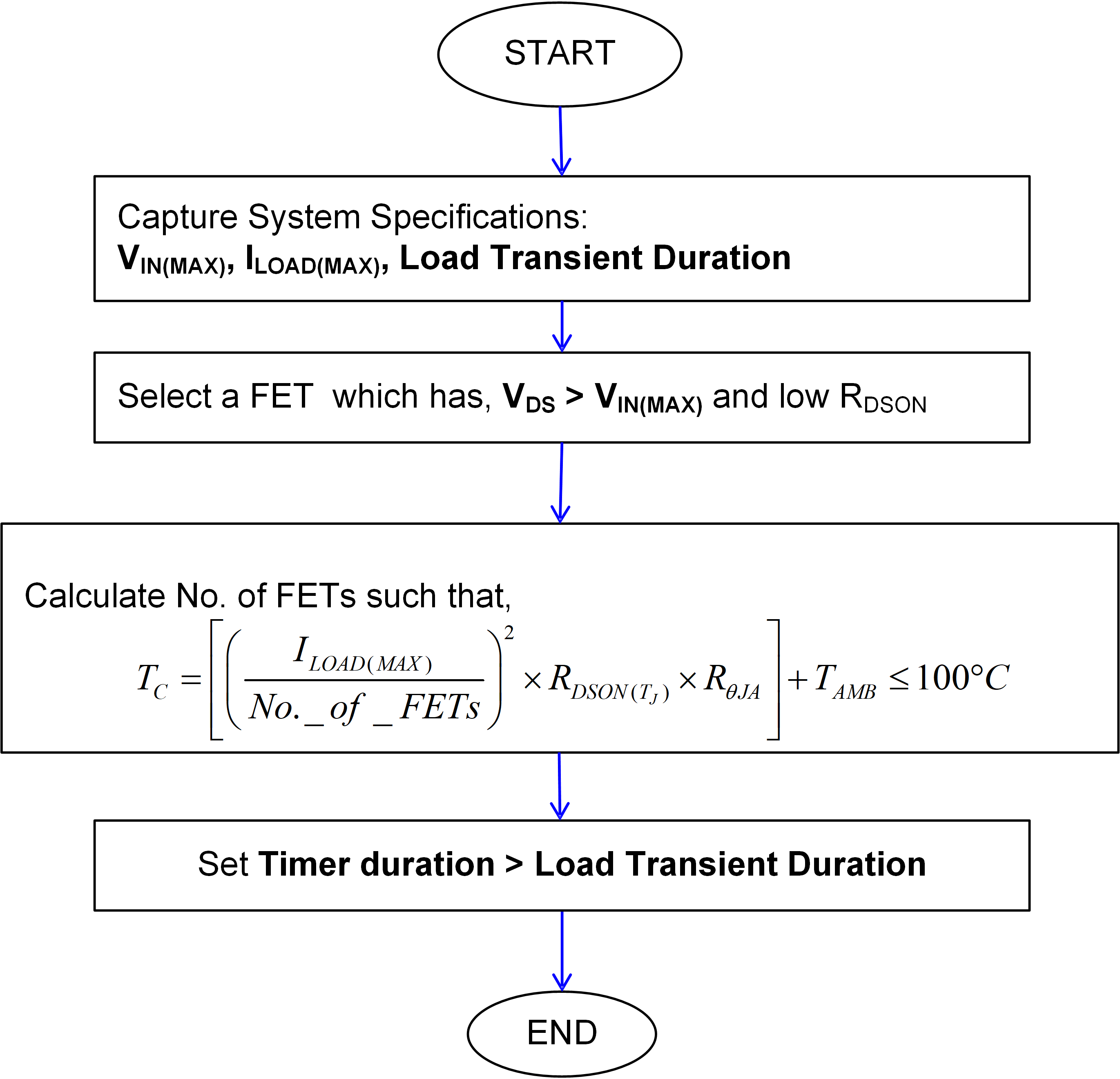
Eliminating the FET SOA greatly simplifies the design procedure with a hybrid hot-swap circuit and a FET with the lowest RDS(ON). The design flow chart for the hybrid hot-swap circuit is shown in Figure 4. For high-current applications, you can simply calculate the number of parallel FETs based on ILOAD(MAX), TAMB(MAX), FET RDS(ON) and RθJA. Choosing a lower RDS(ON) FET can reduce the number of FETs required in parallel, saving board space and reducing solution cost. Since the eFuse manages startup, you can set the timer duration solely based on the load transient duration.
Hybrid hot-swap circuit test results
The advantages of a hybrid hot-swap circuit over a traditional hot swap circuit become more significant when you realize that the power rating of the design increases. To easily understand these advantages, consider two test conditions: startup into a capacitive load and startup into an output short-circuit fault.
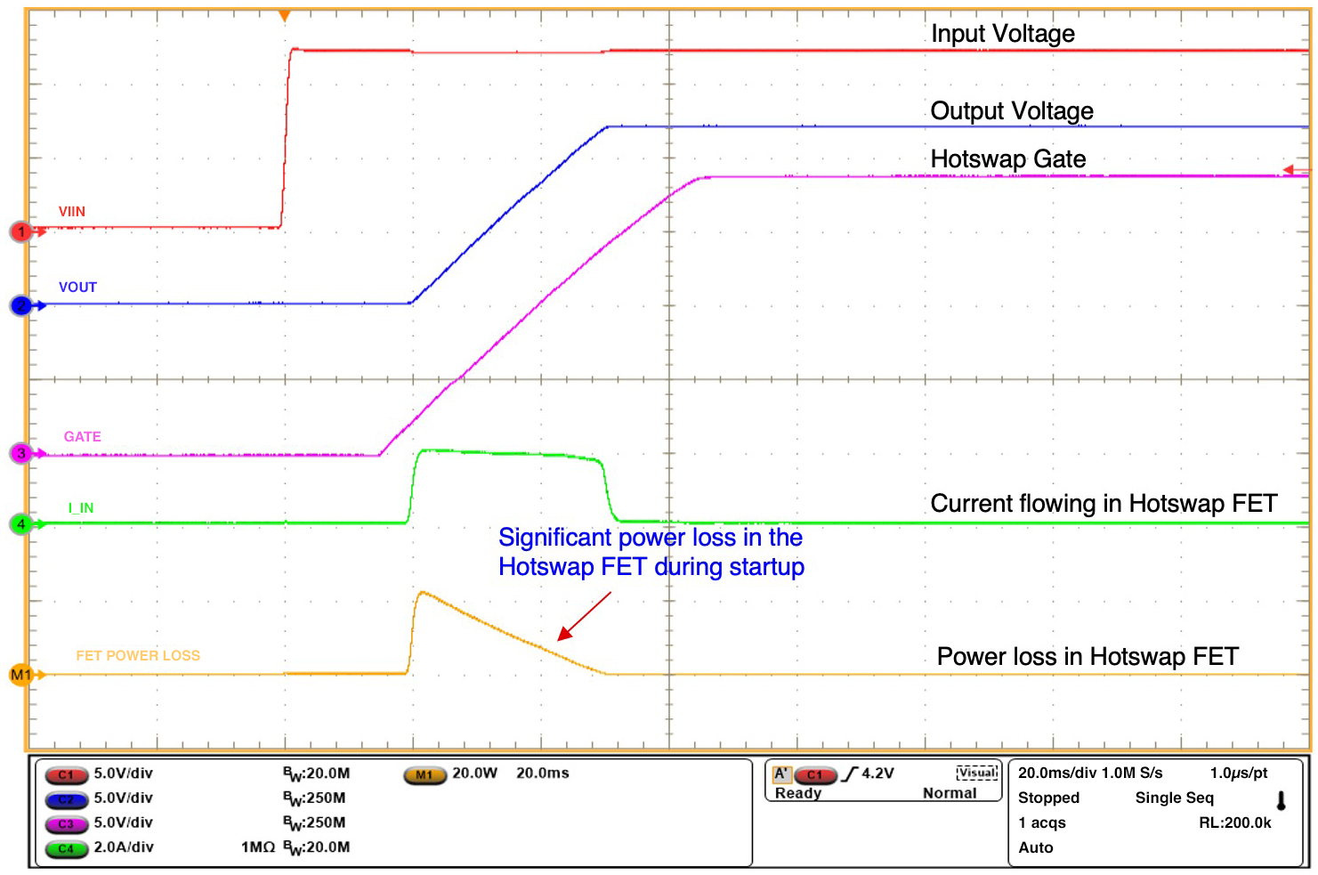
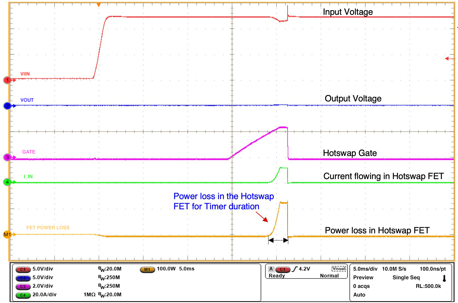
Figure 5 shows the waveform capture of a traditional hot-swap circuit during dv/dt startup into output capacitance. The math function signal in the waveform shows the power loss in the FET during startup. For higher output capacitance values, the power loss in the FET exists for longer durations, making it challenging for the FET to operate within its SOA. Similarly, Figure 6 shows startup into an output short-circuit fault waveform for a traditional hot-swap circuit. You can see that the FETs are stressed for the timer duration before the controller turns the FETs off, proving that FET SOA is a critical design parameter in a traditional hot-swap circuit, as the FET is stressed in different conditions.
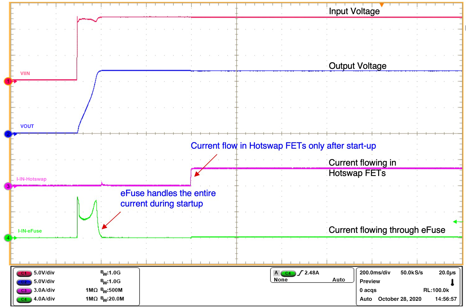
Figures 7 and 8 show the waveform captured for the same test conditions with a hybrid hot-swap solution. Because the hot-swap controller is not enabled until the eFuse ramps the output voltage up to the input voltage, there is no current flow through the hot-swap FETs, and thus no power loss in them. The eFuse with integrated thermal protection handles the stressful events and keeps the hot-swap FETs completely free from SOA limits, thereby simplifying circuit design procedures.

Designing an input hot-swap protection circuit is no longer a headache. Implementing a hybrid hot-swap circuit can make your life easier by eliminating a complex design process while ensuring robust protection along with reduced solution size and cost. For a more detailed description on circuit functionality, advantages, design calculations, and test results of a hybrid hot-swap circuit, see the Texas Instruments Analog Design Journal article, “Protect Against High-Current Faults Using Hybrid Hot-Swap Architecture.”


Leave a Reply