
Power devices based on gallium nitride (GaN) are rapidly becoming a viable, higher-performance alternative to silicon MOSFETs due to their higher efficiency and other favorable attributes.
In recent years, discrete power-switching and power-handling devices based on gallium nitride (GaN) material have become practical and available, and these devices are now found in many power supplies and regulators, usually in the 10-20 A and higher range. This FAQ will look at the basic functional principles of these devices and the rationale for using them, as well as issues related to their application.
Q: What is a power-switch function with respect to a power supply?
A: Today’s power supplies, with some exceptions, are switching power supplies designed using any one of a wide choice of topologies. Regardless of topology, switching supplies regulate their output to maintain the desired output voltage by switching that output rapidly on and off, then filtering this output to provide a steady rail. This switching frequency is usually between 25 kHz to several MHz, with higher frequencies the trend to their smaller sizer (but also having some negatives) losses, in general. As the on/off frequency is usually fixed (in some designs, it is varied), the regulation is achieved by adjusting the duty cycle of the switching action at the nominal operating frequency. (The alternative to a switching supply is the linear supply, which uses a very different approach.)
Q: What makes a good power-switch element?
A: A good switch element has two attributes, which are of primary interest. First, its on-resistance RDS(ON) should be low to minimize IR losses when the switch is on. Second, the losses during the switching period should also be low. These losses are related partially to how fast the device switches from on to off and the reverse.
Q: What switch element have regulators used until recently?
A: In most cases, it’s been a silicon-based MOSFET device. These are available with rating to hundreds and thousands of volts, capable of handling a few amps to hundreds of amps. The on-resistance specifications for most MOSFETs are typically between a few milliohms and about a hundred milliohms.
Q: Why is an alternative needed to silicon-based MOSFETs?
A: There are ever-greater demands now on efficiency, power delivery, supply size, operating temperature, and other factors, to a point where silicon is “hitting a wall” in performance. While there has been progress in silicon devices, the rate of progress is slowing down as the technology is reaching fundamental limits of silicon-device physics (previous advances were primarily related to overcoming imperfections which prevented the silicon devices from reaching their theoretical performance limit).
Q: What’s the alternative?
A: There are two viable alternatives: GAN on a silicon substrate, and silicon carbide (SiC). Both have been under development for decades due to many difficulties to overcome to become practical switching devices. Both GaN and SiC are called wide bandgap (WBG) materials. This FAQ will focus only on GaN devices. (Also note that the engineering community has a longer experience record with GaN due to its use in LEDs.).
Q: Why is it called a wide bandgap material?
A: The bandgap is the energy required for an electron to jump from the top of the valence band to the bottom of the conduction band within the semiconductor. Materials which require energies typically larger than one or two electron-volts (eV) are referred to as wide bandgap materials.
Q: What is special about WBG materials?
A: In brief, it’s this: a GaN switching device is a high electron mobility transistor (HEMT), as shown in Figure 1, with a higher critical electric field strength than silicon, so a GaN device will have a smaller size for a given on-resistance and breakdown voltage than a silicon semiconductor. GaN also offers extremely fast switching speed and excellent reverse-recovery performance, critical for low-loss, high-efficiency performance. (This fast switching is also needed for power supplies which deliver precisely timed, synchronized driving of high-power LEDs in automotive LIDAR systems.)
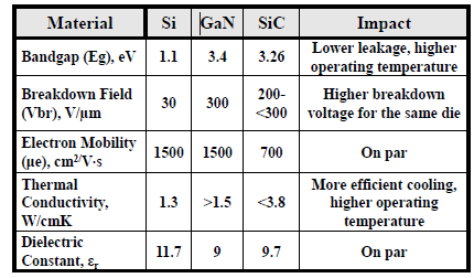
Q: Can you compare the key physics specifications of silicon, GaN, and SiC materials?
A: Figure 1 is a summary of the key specifications and differences.
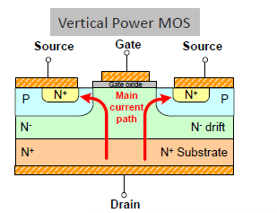
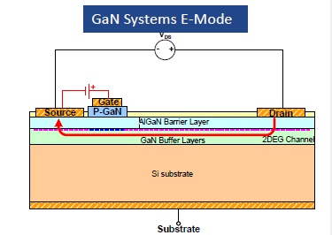
Q: What is the typical structure of a silicon device compared to a GaN device?
A: Figure 2 and Figure 3 show the typical structure of a silicon device and a GaN device; some GaN variations do not have the inherent body diode, which can cause operational difficulties and limit performance.
Q: Do GaN devices come in different variations?
A: Yes, there are two broad types of GaN devices. The depletion-mode GaN transistor is normally on; to turn it off, a negative voltage relative to the drain and source electrodes is needed. The enhancement-mode (e-mode) GaN transistor is the opposite, as it is normally off and is turned on by positive voltage applied to the gate.
Q: What are the implications of these differences?
A: The difference is more than just a matter of their complementary operating modes. The depletion-mode device has a start-up issue in that a negative bias must first be applied to the power device to turn it off and so avoid a start-up short circuit. As a result, depletion-mode GaN devices are often packaged in a cascade configuration with a low-voltage silicon MOSFET that reverses this situation and puts them in a normally-off configuration. In contrast, enhancement-mode devices do not conduct current when there is zero bias on the gate, which is the preferred start-up mode.
Q: All this “device physics” is interesting, but I need more insight if I want to design using a GaN device. What are some similarities between MOSFET and GaN devices? What are some application issues?
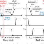
A: The terminology and top-tier parameters are the same: like a MOSFET, a GaN transistor has a source, drain, and gate, and the key figures of merit are on-resistance and breakdown voltage. Further, both MOSFETs and enhancement-mode GaN devices are normally off and are voltage-driven devices (not current-driven) with an input capacitance that must be properly charged/discharged by their driver. The slew rate and shape of this charge/discharge drive waveform is an important factor in performance.
Q: What about key differences?
A: First, GaN’s on-resistance RDS(ON) is very low, thus reducing a major source of static IR losses and inefficiency when in the on state. Also, the GaN FET device has a very low input capacitance, which is key to its faster on/off switching. A GaN device can switch hundreds of volts in nanoseconds, which enables the design of supplies that can switch large currents at rates of several megahertz; this, in turn, can result in higher overall efficiency as well as smaller supply footprint due to smaller magnetics and passive components.
Q: What is the other part of the GaN story, in terms of design-in?
A: As with MOSFETs, the device driver is critical to a successful design. We’ll look at this in Part 2.
Recent GaN products at EE World Online
- “Demo: Gate drivers and eGaN transistors on the same chip”
- “How eGaN transistor technology improves Lidar performance”
- “Rad-tolerant PWM controller/GaN FET driver first to come in a plastic package”
- “eGaN FET gets automotive AEC Q101 qualification”
- “100-V eGaN FETs target 48-V dc-dc conversion”
- “GaN E-HEMT transistors handle 150 A/650 V for EV, energy storage”
- “GaN power transistors cover 3.5-A to 11-A range”
- “Automotive-qualified GaN power FETs work at higher temps than silicon counterparts”
- “AEC-qualified eGaN FETs boost performance in Lidar, automotive systems”
- “GaN 600 V e-mode HEMTs now in volume production”
- “GaN-based, high-power conversion devices target servers EV, industrial equipment“
- “GaN 600-V 50-mΩ/70-mΩ power stages support 10 kW applications“
General References
- APEC/ARPA, “A Pathway to Commercialization of Wide Bandgap Semiconductors in Power Electronics”
- Richardson/Microsemi, “Gallium Nitride (GaN) versus Silicon Carbide (SiC)InThe High Frequency (RF) and Power Switching Applications”
- GaN Systems, “SiC vs GaN Head-to-Head Performance Comparison”
- GaN Systems, “System Level Considerations with GaN Power Switching-Preface”
- Efficient Power Conversion, “Technical Characteristics of GaN and SiC”
- APEC/Transphorm, “Compound Semiconductors; GaN and SiC, Separating Fact from Fiction in both Research and Business”
- Texas Instruments, “Applying SiC and GaN to high-frequency power”
- Texas Instruments, “LMG1205 data sheet”


[…] has released JEP198, a new guideline document for assessing the reliability of Gallium Nitride (GaN) power conversion devices. The document, crafted by the JC-70.1 Gallium Nitride Subcommittee, is […]