Part 1 of this FAQ explored the basics of GaN switching transistors at the device and physics level. This part will look at driving and applying GaN devices.
Q: What do I need to know to use a GaN device?
A: There are three functional blocks associated with power switching: the power-device driver, the power device itself (here, a GaN device), and the load. In most cases, the designer has little control over the load; and selects a GaN device with satisfactory voltage, current, and on-resistance ratings (among other parameters). The remaining challenge, and it can be a large one, is to drive the GaN device properly.
Q: Is this difficult?
A: As usual, yes and no. On one side, a GaN device is functionally similar to the MOSFET, so there’s lots of experience and know-how for driving it. On the other side, the GaN device has some unique attributes and so requires a driver which is properly matched to the device input and switching.
Q: What are some of the requirements a power-device driver, whether GaN or MOSFET?
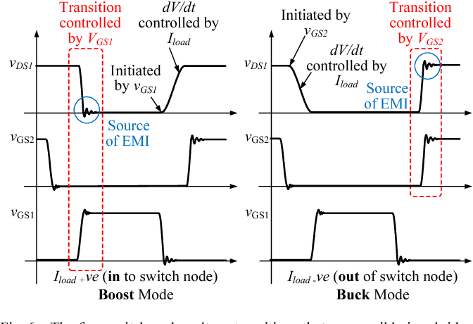
A: The driver must supply the needed current at a high-enough DI/dt rate to quickly charge the input capacitance at the gate of the device and to turn it on, and it must do this crisply without ringing or overshoot. When turning the device off, it must quickly and cleanly “pull” stored charge from the gate input, again without ringing or overshoot. It must also do this with well-defined skew-time control to avoid causing short-circuits due to “shoot-through” in the commonly used bridge configurations, Figure 1.
Q: What issues define the driver function?
A: There are three factors to consider: the maximum allowable gate voltage, the gate threshold voltage, and the body-diode voltage drop (I there is a body diode). Note that the gate-source voltage for an enhanced GaN device is 6V, roughly half that of a MOSFET, which simplifies generating the needed turn-on/turn-off voltages and currents. The gate voltage also has a lower negative temperature coefficient compared to MOSFETs, which also simplifies driver-related temperature-compensation issues (you can not ignore those). Finally, the forward-voltage drop of the body diode (if there is one) is about a volt higher than comparable silicon MOSFETs.
Q: So far, this seems straightforward, is there more?
A: Of course. There is also an inherent Miller-effect charge that limits turn-on/turn-off speed and affects the driver waveform shape. Fortunately, the total Miller charge for a GaN device is much lower than it is for a MOSFET with comparable RDS(ON), easing GaN device turn on/off.
Q: Looks like I can build my own gate driver. Is this feasible?
A: Probably not. Designing and implementing a mediocre gate driver is not hard, but creating a really good one or even a fairly good one is hard. There are many subtleties related to how the current is sourced into the GaN gate and how it is sunk (pulled out), and a circuit made of discrete components would have difficulty addressing these. A good gate driver also has various protection features and ensures the system and power device is not damaged even if there is a short circuit or overheating. These features are costly and difficult to implement effectively with a discrete device design, as that would require more components, and it would have tolerance-buildup, temperature-coefficient, and other issues, and more.
Q: What’s the answer?
A: The answer is not surprising: use a standard GaN driver from one of many vendors. Some of these drivers are from vendors of the GaN devices and so are claimed to be optimally matched, but most are from vendors with experience in providing ICs which are optimized for current sourcing, sinking, and management. Among the many driver vendors are Analog Deices, Maxim Integrated, Silicon Labs, ST Microsystems, and Texas Instruments. These drivers typically include the basic driver function but also add various forms of driver and device protection. They also allow the user to set some key parameters such as source and sink current (which may differ), as well as slew rate to match the GaN device.
Q: Can you give an example?
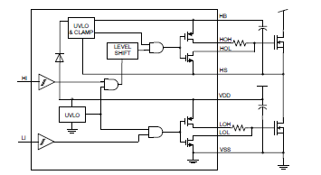
A: The LMG1205 from Texas Instruments (Figure 2) is a gate driver for enhancement-mode GaN FETs. This IC can drive two GaN devices, which is needed for the high-side and the low-side devices in a synchronous buck, boost, or half-bridge configuration. Peak source-current capability is 1.2 A, while peak sink current is 5 A. It also features split-gate outputs for the flexibility needed to independently adjust the turn-on source and turn-off sink currents.
Q: Is the design-in and use of GaN devices still in its infancy?
A: No, not at all. There are many standard power supplies and regulators on the market right now which use GaN devices. Although the GaN power device may be more costly on the BOM compared to a MOSFET of comparable power ratings, the system-level benefits of GaN devices make them the preferred choice in many situations due to their higher efficiency (reduced direct operating cost for power, plus lower cooling costs) , smaller overall circuit footprint, and enhanced performance.
Q: Who makes GaN devices?
A: There are two groups of vendors: established broad-line power-device vendors who realize that GaN is a critical power technology for many present and future applications such as EVs/HEVs and data/farm/server power subsystems; and companies – some of which are relatively new start-ups – who feel they have a unique IP for designing and implementing and fabricating GaN devices while not being constrained by MOSFET-centric thinking or processes. There are at least a dozen sources in each group, giving users a choice: some feel a vendor of MOSFETs and GaN devices can provide an unbiased perspective on which one make more sense; others feel that a GaN-only supplier is really the best source of GaN-optimized products and support.
This FAQ has provided an overview of GaN-device features functions, and benefits, as well as issues associated with using GaN power devices. The references – and there are many other ones available – provide much more information from a variety of perspectives.
Recent GaN products at EE World Online
- “Demo: Gate drivers and eGaN transistors on the same chip”
- “How eGaN transistor technology improves Lidar performance”
- “Rad-tolerant PWM controller/GaN FET driver first to come in a plastic package”
- “eGaN FET gets automotive AEC Q101 qualification”
- “100-V eGaN FETs target 48-V dc-dc conversion”
- “GaN E-HEMT transistors handle 150 A/650 V for EV, energy storage”
- “GaN power transistors cover 3.5-A to 11-A range”
- “Automotive-qualified GaN power FETs work at higher temps than silicon counterparts”
- “AEC-qualified eGaN FETs boost performance in Lidar, automotive systems”
- “GaN 600 V e-mode HEMTs now in volume production”
- “GaN-based, high-power conversion devices target servers EV, industrial equipment“
- “GaN 600-V 50-mΩ/70-mΩ power stages support 10 kW applications“
General References
- APEC/ARPA, “A Pathway to Commercialization of Wide Bandgap Semiconductors in Power Electronics”
- Richardson/Microsemi, “Gallium Nitride (GaN) versus Silicon Carbide (SiC)in the High Frequency (RF) and Power Switching Applications”
- GaN Systems, “SiC vs GaN Head-to-Head Performance Comparison”
- GaN Systems, “System Level Considerations with GaN Power Switching-Preface”
- Efficient Power Conversion, “Technical Characteristics of GaN and SiC”
- APEC/Transphorm, “Compound Semiconductors; GaN and SiC, Separating Fact from Fiction in both Research and Business”
- Texas Instruments, “Applying SiC and GaN to high-frequency power”
- Texas Instruments, “LMG1205 data sheet”




[…] A: As with MOSFETs, the device driver is critical to a successful design. We’ll look at this in Part 2. […]