
Gate drive transformers are often a good solution for providing galvanic isolation in high-voltage and high-frequency applications where fast and accurate signal timing is critical. A gate drive transformer is optimized to handle fast-rising and fast-falling rectangular pulses to turn power switches “on” and “off” in switching power converters. Although many gate drive transformers have 1:1 turns ratios, others are used to step-up the drive voltage as needed for the specific application. This FAQ will start by reviewing general gate drive transformer characteristics, then look at how coupled inductors can be used as gate drive transformers, it will than review single-ended and double-ended transformer gate drives and close by considering the specific drive needs of silicon-carbide (SiC) power semiconductors.
The size of the gate drive transformer is determined by how much drive power is needed to effectively control the power switch. So, the first specification to consider for a gate drive transformer is the volt-time product (V-µsec) rating. To avoid core saturation, the V-µsec rating must be at least as large as the highest anticipated volt-time product in the application. Standard gate drive transformers are available in a variety of form factors that can support a range of V-µsec needs (Figure 1).
Additional key specifications for gate drive transformers include: the dielectric isolation voltage between the gate-to-drive windings (3,750Vrms is often specified), the current rating, the leakage inductance, the DC resistance (DCR) of each winding, the winding capacitances, the common-mode transient immunity, and the operating frequency range. Most standard gate drive transformers have been approved to international safety standards. A transformer-coupled gate drive is often a good option to use for high power applications for several reasons:
- Designs with multiple galvanically isolated output windings can drive all the switches in a bridge circuit and can also make it easier to drive paralleled MOSFETs or IGBTs;
- Gate drive transformers have a negative gate bias when the switch is “off” which reduces dv/dt susceptibility, minimizing the possibility of an excessive dv/dt rate damaging the switching device or causing false switching;
- It can handle high peak currents with power ratings ranging from mW to several kW, and;
- Gate drive transformers have negligible delays and can operate effectively across high voltage potentials.
Coupled inductors
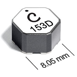
A coupled inductor is simply two or more windings on a common core. They are made in a variety of sizes, inductance values and current ratings with low DCR values (Figure 2). They are often magnetically shielded to prevent electromagnetic interference (EMI). The inductors may have equal or unequal turns ratios and the windings can be used as common mode chokes or as an isolation transformer. When used as an isolation transformer, coupled inductors can be employed as gate drive transformers.
The efficacy of the winding coupling, called the coupling coefficient ‘k’, is determined by the core material used and the structure of the windings and core. Close coupling (k > 0.9) reduces leakage inductance and provides widest usable frequency bandwidth and the most efficient energy transfer. Properly designed, coupled inductors can also provide high voltage isolation between the windings.
The basic circuit
The basic circuit of a transformer-based isolated gate drive is relatively large (that’s one reason for using optocouplers or digital isolators in some applications). In addition to the transformer, the basic circuit includes several “reset” components including a blocking capacitor, primary and gate resistors, back-to-back Zener diodes, and so on (Figure 3).
The blocking capacitor in series with the primary winding of the transformer provides the negative bias, reset voltage, for the magnetizing inductance. Without the blocking capacitor, there could be a duty-ratio-dependent DC voltage (DC offset) across the winding and the transformer could go into saturation. This approach works well where the frequency is high and the duty ratio is relatively small. For duty ratios of 50% or more, a more complex solution is required (and is reviewed in the next section). Core saturation limits the applied V-µsec across the windings. The transformer design must consider the maximum V-µsec under all operating conditions, especially the worst-case transients with maximum duty ratio and maximum input voltage at the same time.
The back-to-back Zener diodes clamp the switch gate voltage, preventing over voltages that can result from the uncoupled transformer leakage inductance. The gate drive resistor controls gate surge currents. Transformer-coupled gate drive circuits are available in single-ended and double-ended topologies. In both cases, the gate drive transformer is are operated in both the first and third quadrant of the B-H plane.
Single-ended transformer-coupled gate drives
In a single-ended transformer-coupled gate drive, a single-output pulse-width-modulated (PWM) controller is used to drive the transformer with pulses that have variable widths and variable amplitudes (Figure 4). This drive circuit is limited to a duty ratio of 50%. For wider duty cycle applications, this circuit cannot deliver adequate gate drive voltage, and a DC clamp, or restoration, circuit has to be added to the secondary side of the transformer using a capacitor and diode. As the duty cycle increases, the coupling capacitor voltage increases, which reduces the actual gate drive voltage (for turn on) and increases the negative bias (during turn off).
Double-ended transformer-coupled gate drives
In a double-ended gate drive circuit, the gate drive transformer is driven with a variable pulse width and constant amplitude from a double-output PM controller to drive 2 or 4 switches in higher wattage converters such as half-bridge and full-bridge topologies (Figure 5). In the figure, OUTA and OUTB are symmetrical and opposite in polarity. When OUTA is on, a positive voltage is applied to the transformer primary winding, when OUTB is on the reverse polarity is applied across the winding. When averaged over two consecutive switching periods, the average voltage across the primary is zero. As a result, a coupling capacitor and damping resistor are not needed on the primary side of the drive circuit.
SiC and CMTI
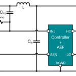
Common-mode transient immunity (CMTI) is measured in kV/µs or V/ns is an important specification when driving SiC MOSFETs. CMTI is a measure of the maximum dv/dt which can be applied across the isolation barrier of the gate driver system before faults occur and cause loss of control of the SiC MOSFET or erratic system opeation. The lower the parasitic capacitance across the isolation barrier, the higher the CMTI. Controlling that parasitic capacitance is critical to controlling the CMTI.
A lower parasitic capacitance results in a lower displacement current for a given level of dV/dt. Too high a displacement current can stress the PWM controller and distort the control signals, resulting in loss of control over the SiC MOSFET. A parasitic (interwinding) capacitance of the gate drive transformer below 7pF can enable the overall gate driver circuitry to achieve CMTI ratings above 100 kV/µs as required by many state-of-the-art SiC applications (Figure 6).
Higher CMTI ratings support faster switching speeds, which is one of the primary advantages of using SiC MOSFETs. Faster switching results in smaller overall solution sizes, lower system costs and improved conversion efficiencies. As a result, the parasitic capacitance across the isolation barrier, which is a combination of the auxiliary supply transformer interwinding capacitance and isolated gate driver IC, should be minimized to realize the very fast switching speed of SiC MOSFETs can achieve.
Summary
Gate drive transformers are optimized to handle fast-rising and fast-falling rectangular pulses to turn power switches “on” and “off” in switching power converters. Key specifications designers need to consider when selecting gate drive transformers include: the V-µsec rating (this is often considered the most important specification), the common-mode transient immunity (this is especially important when driving SiC MOSFETs), the dielectric isolation voltage rating, the current rating, the leakage inductance, the DC resistance (DCR) of each winding, the winding capacitances, the operating frequency range, and whether or not the transformer has been approved to international safety standards.
References
6 W Isolated auxiliary power supply for SiC-MOSFET gate driver, Würth Elektronik
A guide to coupled inductors, Coilcraft
Gate Drive Circuitry for Power Converters, ScienceDirect
Gate Drive Transformers and Circuits, Talema Group
What is a gate drive transformer?, Coilcraft


Leave a Reply