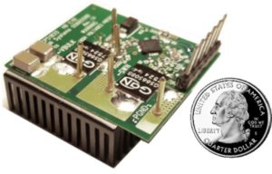
 GaN Systems and ON Semiconductor announced the availability of a high-speed, half-bridge GaN daughter board using GaN Systems’ 650 V, 30 A GaN E-HEMTs and ON Semiconductor’s NCP51820 high-speed gate driver evaluation board.
This evaluation board is developed for existing and new PCB designs and allows designers to easily evaluate GaN in existing half−bridge or full−bridge power supplies. The kit has a reduced component count in an ultra-small 25mm x 25mm layout, minimizing PCB board space. Features, which include 1+ MHz operation and a 200 V/ns CMTI rating, provide increased power density and improved performance with fast-switching GaN power transistors.
Benefits include significant reductions in power losses, weight, size (up to 80% in layout size), and system costs (up to 60% BOM cost savings) and ideal in applications such as AC- DC adapters, data center power supplies, PV inverters, energy storage systems, and Bridgeless Totem Pole topologies. This solution is one of many upcoming GaN-based power system solutions both companies are developing.


thank you for the information