• Skip to primary navigation
  • Skip to main content
  • Skip to primary sidebar
  • Skip to footer
  • Subscribe
  • Advertise

Power Electronic Tips

Power Electronic News, Editorial, Video and Resources

  • Products
    • Power Supplies
    • AC-DC
    • DC-DC
    • Battery Management
    • Capacitors
    • Magnetics
    • MOSFETS
    • Power Management
    • RF Power
    • Resistors
    • Transformers
    • Transistors
  • Applications
    • 5G
    • AI
    • Automotive
    • EV Engineering
    • LED Lighting
    • Industrial
    • IoT
    • Wireless
  • Learn
    • eBooks / Tech Tips
    • EE Training Days
    • FAQ
    • Learning Center
    • Tech Toolboxes
    • Webinars & Digital Events
  • Resources
    • Design Guide Library
    • Digital Issues
    • Engineering Diversity & Inclusion
    • LEAP Awards
    • Podcasts
    • White Papers
    • Design Fast
  • Video
    • EE Videos & Interviews
    • Teardown Videos
  • EE Forums
    • EDABoard.com
    • Electro-Tech-Online.com
  • Engineeering Training Days
  • Newsetter Subscription

Half-bridge power stage delivers Rds(ON) down to 8.05 mΩ

October 15, 2020 By Redding Traiger

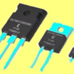
Vishay Intertechnology introduced a new 40 V n-channel MOSFET half-bridge power stage that delivers increased power density and efficiency for white goods and industrial, medical, and telecom applications. Integrating high side and low side MOSFETs in one compact PowerPAIR 3.3 mm by 3.3 mm package, the Vishay Siliconix SiZ240DT provides best in class on-resistance and on-resistance times gate charge — a key figure of merit (FOM) for MOSFETs used in power conversion applications.

The two TrenchFET MOSFETs in the SiZ240DT are internally connected in a half-bridge configuration. The SiZ240DT’s Channel 1 MOSFET, which is typically used as the control switch in a synchronous buck converter, provides maximum on-resistance of 8.05 mΩ at 10 V and 12.25 mΩ at 4.5 V. The Channel 2 MOSFET, which is typically a synchronous switch, features on-resistance of 8.41 mΩ at 10 V and 13.30 mΩ at 4.5 V. These values are up to 16 % lower than those of the closest competing products. When combined with a low gate charge of 6.9 nC (Channel 1) and 6.5 nC (Channel 2), the resulting on-resistance times gate charge FOM is 14 % lower than the next best device, enabling higher efficiency for fast switching applications.

65 % smaller than dual devices in 6 mm by 5 mm packages, the dual MOSFET released today is one of the most compact integrated products on the market. It provides designers with a space-saving solution for motor control in vacuum cleaners, drones, power tools, home/office automation, and non-implantable medical devices, in addition to half-bridge power stages for synchronous buck DC/DC converters, wireless chargers, and switch-mode power supplies in telecom equipment and servers.

The integrated MOSFET features a wire-free internal construction that minimizes parasitic inductance to enable high-frequency switching and thus reduces the size of magnetics and final designs. Its optimized Qgd / Qgs ratio reduces noise to further enhance the device’s switching characteristics. The SiZ240DT is 100 % Rg- and UIS-tested, RoHS-compliant, and halogen-free.

Samples and production quantities of the new dual MOSFET are available now, with lead times of 12 weeks for large orders. Pricing for U.S. delivery only starts at $0.38 per piece.

You may also like:

  • PVs
    Solar systems’ maximum power point trackers
  • GaN MOSFETs
    Boosting efficiency in fast-charge adapters
  • supercapacitors
    Supercapacitor system design considerations
  • littelfuse
    Why it’s tough to characterize SiC power MOSFETs

  • What’s the difference between a MOSFET and a JFET?

Filed Under: ac power sources/frequency converters, Converters, DC-DC, Industrial, Medical, MOSFETS, Motors and motor control, Power Management, Telecommunications, Wireless Tagged With: vishayintertechnology

Primary Sidebar

Featured Contributions

Meeting demand for hidden wearables via Schottky rectifiers

The case for vehicle 48 V power systems

GaN reliability milestones break through the silicon ceiling

Developing power architecture to support autonomous transportation

What makes SiC tick?

More Featured Contributions

EE LEARNING CENTER

EE Learning Center

EE TECH TOOLBOX

“ee
Tech Toolbox: Internet of Things
Explore practical strategies for minimizing attack surfaces, managing memory efficiently, and securing firmware. Download now to ensure your IoT implementations remain secure, efficient, and future-ready.

EE ENGINEERING TRAINING DAYS

engineering
“power
EXPAND YOUR KNOWLEDGE AND STAY CONNECTED
Get the latest info on technologies, tools and strategies for EE professionals.
“bills

RSS Current EDABoard.com discussions

  • Does mobility carrier ratio changes with Wn? (0.18um) inverter design
  • Battery sensing circuitry for coin cell application
  • RF-DC rectifier impedance matching
  • Lightbox circuit help
  • Replacement of the rectifier diode with a MOSFET transistor?

RSS Current Electro-Tech-Online.com Discussions

  • Telegram Based Alarm - Sensor cable protection
  • using a RTC in SF basic
  • 100uF bypass Caps?
  • Lightbox circuit
  • how to work on pcbs that are thick

DesignFast

Component Selection Made Simple.

Try it Today
design fast globle

Footer

EE World Online Network

  • 5G Technology World
  • EE World Online
  • Engineers Garage
  • Analog IC Tips
  • Battery Power Tips
  • Connector Tips
  • DesignFast
  • EDA Board Forums
  • Electro Tech Online Forums
  • EV Engineering
  • Microcontroller Tips
  • Sensor Tips
  • Test and Measurement Tips

Power Electronic Tips

  • Subscribe to our newsletter
  • Advertise with us
  • Contact us
  • About us

Copyright © 2025 · WTWH Media LLC and its licensors. All rights reserved.
The material on this site may not be reproduced, distributed, transmitted, cached or otherwise used, except with the prior written permission of WTWH Media.

Privacy Policy