
Cutting-edge power device technologies all have a niche. Here’s a rundown on the applications in which each one likely fits.
Dr. Gerald Deboy, Dr. Peter Friedrichs Infineon Technologies
The process of converting electrical power to different ac and dc levels and to mechanical motion has changed dramatically over the years. The development of “switched-mode” techniques has been among the most disruptive changes. Switched-mode techniques exponentially boost power conversion efficiency and make practical developments such as isolated dc-dc conversion without motor-generator sets.
Semiconductor switches are, to a large degree, what makes switch-mode conversion possible. Today we have a wide range of power switches from which to choose. They include IGBTs (insulated-gate bipolar transistors) and silicon MOSFETs, as well as wide-bandgap devices based on both silicon carbide (SiC) and gallium nitride (GaN). The application determines which technology may be more reliable, efficient and economical. Design engineers choosing a power switch must evaluate each device’s operating range, properties, challenges and benefits, as well as specific application needs.
Searching for the ideal switch
Power converters are becoming a focal point for saving energy, lowering costs and minimizing environmental impact. High-efficiency converters also bring smaller, lighter and cheaper products without a power consumption penalty and deliver more power in the same volume for the same temperature rise. Power density is also an important metric in applications such as cellular infrastructure, EV/HEVs and edge computing.
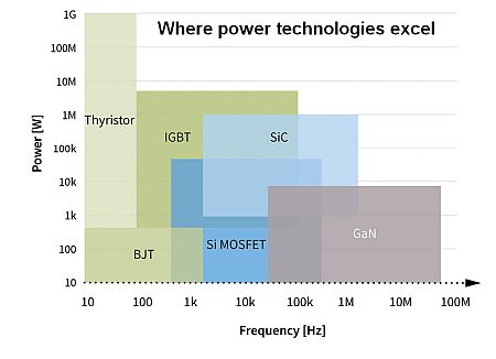
 When evaluating power switches, many believe wide bandgap semiconductors based on SiC and GaN are ideal. GaN seems to be the clear winner in applications requiring a 650-V blocking voltage while SiC is superior above 1,000 V. However, practical components have several qualities that may affect their performance in specific uses. In many applications the latest-generation Si MOSFETs, with lower blocking voltages and high-voltage IGBTs, may cost less and perform better.
GaN is best for new designs. Simply replacing IGBTs or Si MOSFETs with GaN devices and adjusting the gate drive probably won’t bring benefits and may just increase EMI. But existing topologies may see benefits from replacing Si IGBTs with SiC. There can be significantly less loss even with no change in either switching frequency or turn-on/turn-off times.
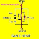
In some applications, the device’s bidirectional capability, or how it operates in its so-called “third quadrant,” is critical. This mode of operation arises when both the drain voltage (collector for IGBTs) and current are negative in n-channel devices, a condition happening under “commutation” in half-bridge networks. This operation mode appears in many common circuits such as inverters, motor drives, totem-pole PFC stages, and the now widely used LLC, phase-shifted bridge and active-clamp flyback converter topologies.
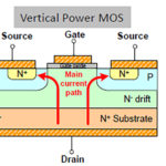
Si and SiC MOSFETs have integral body diodes that conduct under these negative current/voltage conditions. These diodes also exhibit a varying voltage drop and reverse recovery currents of differing amplitudes and durations. However, IGBTs have no intrinsic diode. As the device switches off, a current “tail” causes high power dissipation. Si MOSFET body diodes have a high reverse recovery charge and are relatively slow, causing losses especially at high frequencies. SiC MOSFETs have a negligible reverse recovery charge, but the diode has a high forward-voltage drop when it conducts, again dissipating energy. Thus, designers increasingly use synchronous rectification (replacing diodes with actively controlled switches) which, in turn, lowers static losses below that when diodes are used in combination with IGBTs.
On the other hand, GaN conducts in the third quadrant with a drop defined by low channel resistance and with no reverse recovery at all. Both effects help minimize power losses. GaN and SiC are, therefore, ideal solutions for optimizing efficiency with half-bridge-based topologies, particularly under “hard” switching conditions. With “soft” or resonant switching, Superjunction Si MOSFETs are still the optimal choice up to about 250 kHz.
Current and voltage ratings also limit GaN applications, making IGBTs and SiC the dominant technologies for higher currents and voltages.
The importance of power density
Although efficiency is key, high power density is sometimes the actual design aim. The maximization of power density involves a choice between high-frequency operation with GaN, potentially reducing the size of passive components, or operating Si or SiC MOSFETs at lower frequencies with slightly larger passive components. SiC and GaN circuitry, with typically better efficiency, allows use of smaller heatsinks. But the thermal design of associated components must be done with care. The selection of topology and control strategies for hard or soft switching (where the voltage or current through the device is zero when it switches) also play important roles.

For example, consider the energy efficiency efforts of the Open Compute Project, where OCP members share designs for data center products. The trend is to integrate power converters into the rack, with projected lifetimes of six to eight years, instead of the typical two-to-three-year life of power supplies mounted directly on motherboards.
At an efficiency level close to 98%, GaN designs pay for themselves after around three years depending on electricity costs. Their reduced converter size and higher efficiency can also allow more server blades to fit in each rack, boosting data throughput.
The same benefits are available in other applications. In motor drives, for example, more efficient GaN technology could substantially reduce inverter temperature rise and allow twice as many drives to sit in a cabinet, greatly reducing the need for expensive factory floorspace.
Figures of merit
The figure of merit (FOM) for a power-handling devise is the product of ON-resistance and die area – RDS(ON)×A. FOM is a good indication of how much power the device handles for a given voltage rating. A low value implies a smaller die with correspondingly smaller device capacitances and higher switching speeds. It also implies more die per wafer for a given power rating, potentially lowering device costs.
A similar FOM given by RDS(ON)×EOSS combines conduction losses with switching loss generated by the dissipation of stored energy, EOSS, in device output capacitance each switching cycle. The lower the FOM, the lower the losses. EOSS itself, the energy stored in device output capacitance, is a similar indicator of turn-on losses. Total gate charge QG(TOT) affects gate drive power PG required, according to:
PG = QG(TOT) × F × VGSW where F = frequency, Hz; and VGSW = gate voltage swing, V.
This relationship is important because gate-drive power can affect system efficiency. GaN has a low threshold voltage of around 1.5 V and extremely low QG(TOT). So gate-drive power is just milliwatts even at high frequencies. On the other hand, IGBTs can require several watts of gate drive, even at low frequencies, because of their typical gate-voltage swings between +16/-9 V and gate charge measured in microcoulombs.
SiC lies between the two. The charging and discharging of the capacitance associated with QG(TOT) through device and external gate resistance also affects switching speed and EMI generated.

How Si-Superjunction MOSFETS have improved over time.
To get a feel for the direction of the trend, consider work underway at Infineon. Infineon aims to move towards ever-better RDS(ON)×EOSS and RDS(ON)×A. Infineon pioneered Si-Superjunction technology and expects to halve the RDS(ON)×A FOM to about 5 mΩcm² in the future. New Trenchstop-based IGBT topologies also improve the VCE_SAT vs. QTOT trade-off. And Infineon continues work on wide bandgap devices as GaN and SiC technologies are still far from the theoretical performance limits for RDS(ON)×A FOM.
All in all, the selection of a solid-state power switch involves device qualities, including TCO, system implications, and performance requirements. Optimal electrical performance will come with ground-up designs using wide bandgap devices.


Leave a Reply