
Enhancement mode (e-mode) GaN high electron mobility transistors (HEMTs) generally behave like n-channel power MOSFETs. Common curve tracers, parametric analyzers, and automatic discrete device parametric testers used for an n-channel power MOSFET can be applicable for the characterization of e-mode GaN transistors, but the implementation details differ for GaN. Typical e-mode GaN HEMTs have very low parasitic components. They switch very fast at high frequencies with short delays. Without proper consideration, the equipment used to perform the tests can introduce parasitics that contaminate the results and lead to incorrect measurements. In addition, possible shortcomings have been identified with the conventional double pulse testing (DPT) results related to the dynamic on-resistance of GaN devices.
This FAQ reviews current industry standards for testing devices fabricated using wide bandgap semiconductors such as GaN, reviews DPT and related test equipment, and closes with a brief overview of a proposed ‘N-pulse’ testing procedure that may provide superior results for GaN devices compared with current DPT procedures.
JEDEC standards have begun to address the need for wide bandgap (WBG) standards for GaN and silicon carbide (SiC) power semiconductors. The JC70 Wide Bandgap Power Electronic Conversion Semiconductor committee includes separate focused sections related to GaN (JC70.1) and SiC (JC-70.2). Each section has three task groups; Reliability and Qualification Procedures (for more information on GaN reliability, check out the FAQ, “How Reliable are GaN HEMTs?”), Datasheet Elements and Parameters, and Test and Characterization Methods. For GaN, there are two current testing standards:
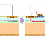
JEP173 – Dynamic on-resistance (RON) test method guidelines for GaN HEMT based power conversion devices, Version 1.0. These are guidelines, not requirements. GaN technology is well established but not completely mature. Dynamic RON is a GaN-related phenomenon and a critical performance parameter. Dynamic RON occurs when the RON increases after being exposed to a drain bias. It’s caused by electrons that get trapped and deplete the 2-dimensional electron gas (2DEG) that acts as the conducting layer in the device. The test outlined in JEP173 is designed to be used on wafers in the fabrication process to determine if devices, sections of the wafer, or the entire wafer are usable.
JEP182 – Test method for continuous-switching evaluation of gallium nitride power conversion devices. JEP182 is intended to supplement the use of power device analyzers to carry out static measurements on GaN HEMTs. Currently, DPT is the preferred procedure for determining the dynamic performance characteristics of GaN devices.
Double Pulse Testing
DPT is used to measure power devices’ switching parameters and dynamic behavior. It’s called double pulse because two pulses are sent to the device under test (DUT) in a clamped inductive load circuit (Figure 1). The DUT’s switching characteristics can be measured under the desired voltage and current conditions at the end of the first pulse and the beginning of the second pulse by regulating the dc bus voltage and first pulse duration.

The circuit conditions in the intended circuit design are replicated by the inductor (L). The power supply (VDC) provides voltage to the inductor. An arbitrary function generator produces the pulses that trigger the MOSFET gate, turning it ON at the beginning of each pulse to start the conduction of current. With only two pulses for each test, the DUT junction temperature increase due to switching losses is negligible. DPT can be used to measure numerous switching parameters, such as:
- Turn-on parameters: Turn-on delay, rise time, turn-on time, dv/dt, and di/dt.
- The corresponding turn-off parameters: Turn-off delay, fall time, turn-off time, dv/dt, and di/dt.
- Reverse-recovery parameters: reverse-recovery time, reverse-recovery current, reverse-recovery charge, reverse-recovery energy, di/dt, and forward on voltage.
There are several subtleties to consider when using DPT that can make it challenging to produce realistic test results:
- The DPT board layout should as closely as possible match the intended converter application, including critical parasitics such as common source inductance, power loop inductance, and so on.
- The probes used to measure the switching waveforms must meet the test’s bandwidth, accuracy, and dynamic range needs.
- Due to the sensitivity of switching losses to V-I timing misalignment, the current and voltage channels must be deskewed.
- For accurate measurement of the high-speed waveforms, probe grounding effects must be suppressed using probe-tip adaptors and common-mode chokes when needed.
Testing equipment
The basic equipment needed to perform a DPT is relatively simple (Figure 2):
- Arbitrary function generator. Some models have a built-in double-pulse application that can generate pulses with specified pulse widths.
- Oscilloscope to measure Id, Vds, and Vgs.
- High common mode rejection probe for measuring Vgs.
- D.C. power supply
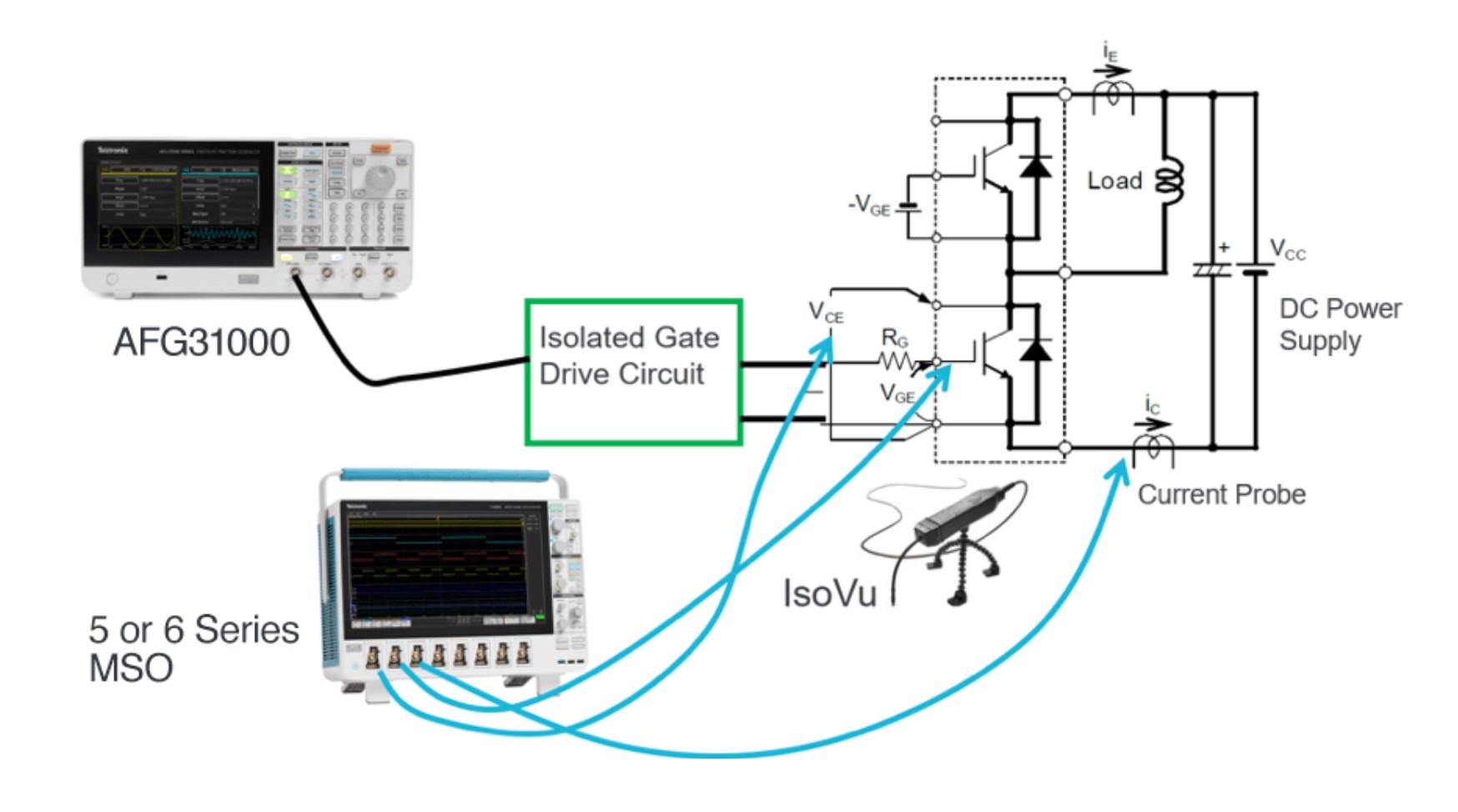
An oscilloscope is used to measure the falling edge of the first pulse and the rising edge of the second pulse to capture the turn-on and turn-off characteristics. With some oscilloscopes, with the falling edge and rising edge waveforms on the screen, turn-on loss can be calculated using standard integrated math functions in the oscilloscope.
Reverse recovery current occurs during the turn-on of the second pulse and produces energy losses, which directly impact the power converter’s efficiency. Initially, the diode is operating in a forward condition. A perfect diode would immediately switch to a reverse blocking condition when the low-side MOSFET turns on again. But a real diode conducts in a reverse condition for a short period, and that current is the reverse recovery current.
In addition to DPT, short-circuit robustness can withstand unintentional fault conditions is important for GaN devices. Under short-circuit conditions, the device will see the full bus voltage plus a current limited by the inherent saturation current of the device and any circuit parasitic resistances. Protection is usually present to quench the short circuit and protect the device from excessive power dissipation and failure. Short-circuit tests are designed to quantify the withstand time a device can survive. Since typical protection circuits can detect and react to short-circuit conditions in 3 μs or less, it is usually required that GaN HEMTs can withstand unclamped short-circuit conditions for at least 5 µs.
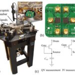
There are dedicated testers that can measure the dynamic RON, switching characteristics, short-circuit robustness, and other performance parameters of GaN HEMTs (Figure 3). These testers are programmable and support standard JEDEC standards and custom testing required for specific application segments such as energy systems or electric vehicles.

Does GaN need more than two pulses?
Standard DPT has proven useful when the DUT is a Si device but may be less useful with GaN HEMTs. To most closely match the results expected in a real-world application when DPT testing of Si devices, the temperature of the DUT must match the expected operating temperature. There are additional concerns when testing GaN devices. They experience electron/hole trapping between the device layers of GaN, AlGaN, and p-GaN, which modulates the gate threshold voltage and produces dynamic RON. To compare alternatives to conventional DPT, a board was designed to operate in continuous mode or DPT mode or the recently-proposed ‘N-pulse test’ (NPT) mode at 2kW (Figure 4).
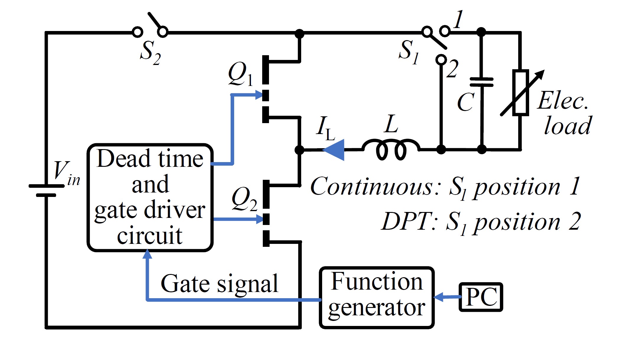
The proposed NPT replaces the initial charging pulse used in a DPT with a series of N equally-sized pulses. The N pulses cumulatively deliver the same current as the initial DPT pulse. To implement NPT, the test is run repeatedly, with each run separated by 1 second rest times until the switching reaches a steady state. For each NPT, an oscilloscope captures the last turn-on edge. Results from ten consecutive NPTs are averaged to arrive at the final result.
A 20PT and a DPT were implemented on GaN devices using the described test setup and methodology with a D.C. link setup time of over 100 seconds for both tests. The 20PT produced significantly better results than a conventional DPT test, with the inferred switching energy of the 20PT matching the actual value to within 4 percent.
Summary
JEDEC and other testing standards for GaN are relatively new and still evolving. There are several current tests that GaN users need to consider, including DPT and short circuit evaluations. Those tests can be implemented with commonly-available laboratory equipment such as arbitrary function generators and oscilloscopes or with dedicated systems in production environments. There is a concern that while conventional DPT is useful for Si-based devices, GaN technology may require new approaches such as NPT to achieve repeatable and accurate test results.
References
Customized GaN Solutions for Double-Pulse Test, Keysight Technologies
Double pulse testing, Tektronix
Investigating GaN power device double-pulse testing efficacy in the face of VTH-shift, dynamic Rdson, and temperature variations, IEEE/University of Bristol
Measurement Techniques for High-Speed GaN E-HEMTs, GaN Systems
Methodology for Wide Bandgap Device Dynamic Characterization, U.S. DoE Office of Science and Technical Information


Leave a Reply