
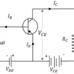
In Part 1 of this FAQ, we looked at the basic DC load line for a simple, basic common-emitter transistor configuration. Part 2 looks at how this graph is used to maintain the linear AC performance of the amplifier configuration.
Note that the term “quiescent mode” or “quiescent state” is also used with ICs and subcircuits to indicate that they are in a minimal-power mode. This is unrelated to the quiescent operating point of the transition and load line but can cause some confusion, especially as an IC in quiescent mode dissipates its least amount of power, while a transistor at its quiescent point dissipates the most power or nearly so. For this reason, many engineers prefer the term “operating point” to avoid confusion.
Q: We have the DC operating points, but how do they affect AC (amplification) operation?
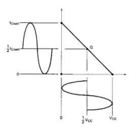
A: Adjusting the base current so that the circuit is at a desired operating point with no signal applied is called biasing the transistor. When using the transistor to amplify an input signal, the input varies around the initial bias-value setting, and so IC and VCE also vary around their initial DC values. It is preferred in most cases to have the quiescent operating point centered on the load line, in which case the amplifier is said to be midpoint biased.
Q: Why is midpoint bias desirable?
A: Midpoint biasing allows optimum AC operation of the amplifier, as it allows IC and VCE to make the maximum possible transitions above and below their initial DC values. This allows maximum gain without affecting the fidelity of the output waveform with respect to the input waveform, Figure 1 and Figure 2.

Q: What else may happen if the biasing is not at midpoint?
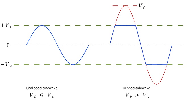
A: When the quiescent operating-point is above the center on the load line, the input signal may cause the transistor to saturate. When this happens, a part of the output signal will be clipped off, Figure 3. When that-point is below midpoint on the load line, the input signal may cause the transistor to cutoff. This can also cause a portion of the output signal to be clipped. The top or bottom of the input AC sine wave will be flattened. If the goal is to maintain amplifier performance with no or low distortion, clipping and cutoff must be avoided,
Q: Are clipping and saturation always bad?
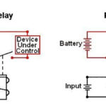
A: No. They are bad if the goal is to amplify the input signal with minimal distortion, added nonlinearity, and other input/output differences other than pure gain. However, if the transistor is to be used as a nonlinear digital switch, whether to generate a binary drive or to control a load such as a relay coil, it may make sense to have the non-activated operating point of the transistor be close to cutoff, with the active engaged state at saturation. This will result in optimum on/off transitions as well as greatly reduced power dissipation.
Q: What is the AC load line?
A: The AC load line is not the same as the DC load line. It is straight line through the quiescent operating point but having slope corresponding to AC load resistance. The AC load seen by the amplifier is different from the DC load, and so the slope of AC load line is different. The AC load line indicates the maximum possible output-voltage swing, called the peak-to-peak output voltage (Vpp) for a given amplifier configuration. This maximum Vpp is often referred to as the compliance of the amplifier.
Q: What is the compliance value?
A: The maximum possible transition for VCE is equal to the difference between VCE when the transistor is off and VCE at the quiescent operating point. Since this transition is equal to quiescent collector current IQ × RC, this is the maximum peak-output voltage from the amplifier. The maximum peak-to-peak transition of the output voltage is twice that voltage value, assuming the amplifier is midpoint biased.
Q: It seems as if this discussion is similar to the discussion of load matching. Is this correct?
A: It’s a little “yes” and mostly “no.” All things in a circuit are related to another thing, since they are all tied together by fundamentals such as Maxwell’s equations, Kirchhoff’s law, and other laws. But these curves and operating points are used in lower-frequency regions to ensure maximum linearity of the amplifier and maximum gain without distortion (unless distortion is not an issue).
On the other hand, impedance matching in RF circuits is needed where there is an amplifier which is already producing a given output power at a certain level of distortion and needed to transfer that power to a load (which can be an antenna (in most cases) or another circuit subsection).
References
- “What are amplifier classes and their relation to power efficiency (Part 1)?”
- “Solenoids and relays, Part 1”
- “Solenoids and relays, Part 2”
- “Impedance matching and the Smith chart, Part 1”
- “Impedance matching and the Smith Chart, Part 2”

Thanks to all of you involved in producing such clearly written text to explain the meanings and usages of all these graphs. I stuck at the a c load line, but now I understand. Thanks once again.