
Part 1 of this FAQ looked at the need for the load-switch function for a circuit’s DC rails, the basic implementation using a MOSEFT and driver, and the limitations of this approach. Part 2 looks at what are referred to as load switches, which in this context means ICs designed to implement the load-switch function, and provide additional features and benefits that these IC designs can offer.
Q: What is an IC load switch?
A: The IC load switch is a small, simple component with allows a basic, low-level digital control line to turn the DC supply rail on and off.
Q: Is the IC-based load switch hard to use?
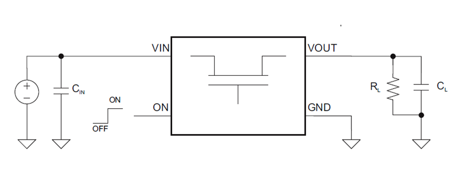
A: No, in fact they are very easy to use. The standard load switch is a four-terminal device, Figure 1, with input rail, output rail, ground, and control. Even though they include the MOSFET and its driver, as well as other circuitry, they are also tiny, commensurate with their four-terminal pinout requirements. Some load switches also require a capacitor on their input and/or output connections.
Q: What else can a load switch IC do?
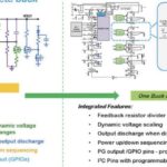
A: They can do lots of things which increases their usefulness yet requires no additional user interaction and has little or no impact on size. They are enhanced with other functions such as discharge control, slew-rate control, various forms of protection, and fault monitoring, Figure 2.

Q: What are some of the other virtues of an IC load switch?
A: There are several:
- The driver within the IC manages the charging and discharging the MOSFET gate, thus providing slew-rate control of the rise/fall times of the MOSFET turn-on/turn-off cycle. This optimizes the MOSFET performance, avoids overshoot and ringing, and minimizes undesirable EMI/RFI.
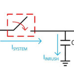
- Further, control of the turn-on time of the MOSFET in the switch prevents the input rail from sagging or drooping due to the sudden increase in load and associated inrush current result from quickly trying to charge the load’s capacitor. This becomes a system problem if that same input rail is also powering other sub-systems which must remain fully powered, as if usually the case.
- Load switches can incorporate other features which are desirable whenever there is a power source and rail, such a thermal shutdown, undervoltage lockout, current limiting, and reverse-current protection. These protection features contribute to system-level integrity.
- Some load switches offer a quick output-discharge feature via an on-chip resistor between the output and ground; this mode is activated when the device is disabled via the ON pin. This will discharge the output node, preventing the output from floating, which can cause unwanted activity the load circuitry is not powered down to a defined state.
Q: Wait a moment: isn’t that last feature is sometimes undesirable? If the output of the load switch is connected to a battery, this quick-output discharge would cause the battery to drain when the load switch is disabled via the ON pin—not a good thing!
A: Yes, that’s true, and therefore some vendors offer it as a selectable feature in a single device, while others offer two variations of their load switch, with one having it and the other not. Problem averted!
Q: What else can be done by leveraging the load switch capabilities?
A: By using an array of load switches, a single larger supply can power multiple circuit subsections, with up/down power to these subsections implemented via a prescribed sequence and timing under the control of multiple digital outputs, Figure 3. In this way, the load switches act as the gating elements of a broader and effective power-management control scheme.

Q: What are the primary parameters of interest when choosing a load switch?
A: They are similar to those of a standard FET used as an on/off switch. These include:
- On-state resistance (Ron) determines the voltage drop across the load switch and allows calculation of the power dissipation of the switch. Typical on-resistance values are around ten milliohms; the designer must do some basic calculations to determine the maximum allowable value in the application;
- Maximum voltage (Vin) and current (Imax) ratings specify how high a voltage the switch can tolerate, and with how much maximum current flow;
- Quiescent current — the current that the load switch consumes when the load switch is on, and thus becomes wasted power – is usually negligible compared to the power that the load itself is dissipating;
- Shutdown current, which is how much current “leaks” from the load switch to the load when the switch is in off mode (not the same as quiescent current);
- Other factors may include package type, available vendors and alternate sources, and special features such as quick-output discharge (or disabling it), a discussed earlier.
The load switch is one of those small, handy, easy-to-use components that can solve many system-level problems, including maximizing run time by saving on battery power, reducing unnecessary thermal dissipation, and managing turn-on/off timing slew rate and multi-rail sequencing. While the load switch may require an input or output capacitor (see the specific device data sheet), that is a modest consideration. They are also very inexpensive and small, both important virtues.
References
- Texas Instruments, SLVA652, “Load Switches: What Are They, Why Do You Need Them And How Do You Choose The Right One?”
- Vishay Intertechnology, Inc, “Smart Load Switches”
Leave a Reply