New gate drivers simplify the task of deploying silicon-carbide FETs to shrink the size and boost the efficiency of power inverters.
Charlie Ice Silicon Labs
The electric vehicle revolution is upon us. Automotive companies search desperately for a technological edge, investors see EV companies as more valuable than traditional automakers, and governments press ahead with ending sales of internal combustion vehicles. Under the hood, the power electronics driving EVs are rapidly evolving as well. Wide bandgap FET technology like silicon carbide (SiC) promise dramatic efficiency improvements, lighter weight systems, and smaller batteries. In automotive designs, SiC is delivering on these promises and driving innovation in the next generation of EVs.
The fundamental advantage of SiC and other wide-bandgap devices can be understood from their bandgap, the energy difference between the top of the valence band and the bottom of the conduction band . Moving electrons from the low-energy valence band to the higher-energy conduction band causes a material to conduct. To move an electron from the valence band to the conduction band in silicon takes 1.1 eV. SiC, on the other hand, has a bandgap of 3.2 eV, so it takes more energy to move the electrons to the SiC conduction band. This fact translates into a much higher breakdown voltage for a given die size than is the case for silicon devices. The SiC die size advantage and benefits such as lower on-resistance (RDSON) and faster switching speed are practically tailor made to solve the biggest EV challenges.
Three of the main limitations of EVs are charge time, range, and cost. Boosting the high- voltage portion of the EV inverter circuit, known as the dc link, to 800 or even 1,000 V lowers the current involved and thus allows lighter-weight cables and magnetics. Higher voltages require switching devices with higher breakdown voltages, often up to 1,200 V. For standard silicon MOSFETs, scaling the breakdown voltage to this level, while maintaining high current capability, is impractical because the necessary die size becomes prohibitive. Bipolar silicon devices, primarily insulated bipolar gate transistors (IGBTs), solve this problem but sacrifice switching speed and limit power conversion efficiency. The wide band gap of SiCs allows unipolar FET devices, with dramatically smaller die sizes, to exhibit the same breakdown voltage and current ratings as traditional IGBTs. This ability brings several improvements to power conversion systems while allowing higher dc link voltages and reducing vehicle weight.
To improve the range of an EV, either the battery capacity must increase, or the vehicle must become more efficient. In general, boosting the battery capacity adds cost, size, and weight, so designers focus instead on improving the efficiency of the vehicle power conversion systems. With the correct switching devices, designers can up the power supply switching frequency as a way to raise efficiency while simultaneously reducing the size of the magnetic components, reducing cost and vehicle weight. In addition, the resulting highly efficient converters need less heat sinking and cooling systems.
SiC FETs naturally accommodate these high switching frequencies because they dissipate little energy in each charge/discharge cycle. Furthermore, the material properties of SiC, combined with the small die sizes, allow operation at higher temperatures with lower losses than IGBTs.
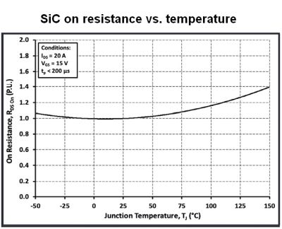
Unlike IGBTs, SiC FETs have an RDSON specification, and the rated RDSON varies little with temperature. This concept is critical for high-power EV applications, where the switching devices handle kilowatts of power and routinely reach high temperatures. In addition, IGBTs are typically optimized for maximum current; their conduction losses rise dramatically at less than maximum load. SiC FETs, however, maintain their efficiency at low loads. This behavior is particularly useful in automobiles, where systems like the traction inverter operate at different loads for long periods.
All of these improvements from SiC FETs add up to greater efficiencies, smaller batteries, lower costs, and ultimately more capable EVs. Nonetheless, the adoption of SiC technology requires designers to learn new techniques, and some of the most important techniques center on the gate driver.
Silicon carbide FETs, with their smaller die size and higher switching frequencies, require slightly different gate drive techniques. The small die size makes SiC FETs more susceptible to damage, and the higher frequencies necessitate a gate driver with improved performance. Finally, SiC FETs often require a higher gate drive signal and a negative gate voltage in the off state. The latest isolated gate drivers integrate the features necessary to meet all these requirements.
Many high-voltage automotive systems use isolation devices, such as isolated gate drivers, to separate the low-voltage controller from the high-voltage portion of the system. The high switching frequencies used in most SiC FET designs subject the isolated gate driver to fast transients. A gate driver with a common-mode transient immunity (CMTI) of at least 100 kV/µsec can withstand these transients. Furthermore, the driver’s propagation delay and channel-to-channel skew generally must be below 10 nsec for the design to be stable at such high speeds. As automotive systems push dc link voltages higher, the isolated gate driver must also have enough maximum insulation working voltage (VIORM). Thanks to technological advances, designers can simply select an isolated gate driver that meets the needs of a SiC FET based system.
Many new isolated gate drivers, such as the Silicon Labs Si828x, also include an integrated Miller clamp and desaturation detection to protect the SiC devices. In a half or full bridge configuration, the switching device on the lower half of the bridge experiences a fast change in voltage on the drain when the upper device turns on. This change induces a current in the gate to drain parasitic capacitance which can otherwise discharge through the gate and turn on the lower device. This “Miller parasitic turn on” causes shoot-through which will quickly damage a SiC device.
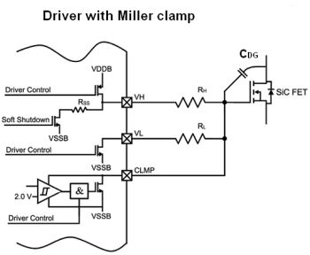
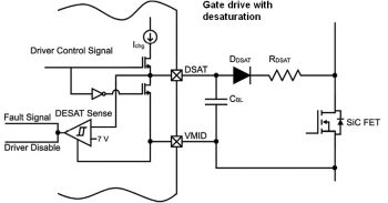
An integrated Miller clamp discharges the gate to drain parasitic capacitance when it reaches a pre-configured threshold. In addition, abnormal load conditions may cause the switching device to fall out of saturation and be damaged. But there is a desaturation circuit integrated into the Silicon Labs Si828x gate driver. If the voltage across the switching device rises above a configured threshold, the gate driver quickly responses and shuts it off gracefully. It does so using a soft shutdown circuit to limit the induced shutdown voltage across the switching device.
In the case of a SiC FET, the protection circuit must react quickly, often in under 1.8 µsec, to be effective. With these three features integrated into the gate driver, it becomes much simpler to design a robust, reliable SiC power converter.
The final aspect of driving SiC FETs is the use of a negative voltage when turning off the FET. The negative voltage works in conjunction with the Miller clamp to secure the FET in the off state, an aspect of operation that is critical in controlling shoot-through current in high frequency power converters. The methods to generate the necessary negative voltage rail are beyond the scope of this article. However, selection of a gate driver with an integrated dc-dc converter generally simplifies the design.
All in all, silicon-carbide switches open the door to faster switching speeds, greater efficiency, and higher power density than ever before. Among other benefits, their high breakdown voltage and thermal performance comprise natural building-blocks for automotive power systems. These advantages, coupled with the improved capabilities of isolated gate drivers, make them core technologies in the electrification revolution.







Leave a Reply