
By, Andrew Berry, Principal Product Modelling Engineer, Nexperia
Many manufacturer-provided simulation models are available for use when designing with discrete power MOSFETs. However, few (if any) accurately represent real-world performance, reducing their use when using tools such as SPICE to simulate practical applications.
Temperature is always a factor in power design, and many models are limited to a single nominal temperature (typically 25 °C) which is not representative of typical performance. These manufacturer-supplied models are often ‘simplified’, neglecting device parameters that will affect important performance areas – such as electromagnetic compatibility (EMC). Unlike engineers who work with complex integrated circuits supplied with comprehensive models, discrete designers often feel ‘short-changed’.
In this article, we will review the restrictions within standard power MOSFET models by simulating a half-bridge stage commonly used in motor control applications. This approach will be contrasted with new, advanced electrothermal models intended to furnish circuit designers with a significantly better insight into how MOSFETs actually perform when mounted on a printed circuit board (PCB) in a real-world application.
Standard model limitations
Prediction of a discrete MOSFET’s dynamic performance (especially switching and EMC) requires a model that simulates the static and dynamic characteristics across the full operating temperature range. Equipped with such a model, simulation packages (such as SPICE) can perform accurate circuit simulations.
As most manufacturer models omit at least some of this information, they cannot be wholly relied upon. As a result, designers have to make reasonable assumptions, erring on the side of caution. While a valid design approach, this can ignore subtle (but important) board-level behaviour, and using worst-case scenarios will almost certainly result in an over-engineered design that is more expensive. Critical performance factors such as EMC cannot be simulated, so they can only be understood once the cost and effort of creating a full prototype have been incurred.
Testing discrete power MOSFETs
When testing MOSFETs and other devices for use in inductive clamp circuits, the industry generally relies upon a technique known as ‘double pulse testing’. This entails using a half-bridge circuit, an inductive load, a low-side MOSFET, and a high-side MOSFET configured to perform the role of a freewheeling diode.
A pair of pulses is injected into the gate of the low-side MOSFET to perform the test. The first pulse operates the MOSFET, allowing current to flow and charge the inductor. When the MOSFET gate signal pulled low, the MOSFET is turned off. At this point, the charge in the inductor causes a current to begin flowing through the body diode of the high-side freewheeling MOSFET. As a result, charge (as reverse recovery charge – Qrr) accumulates in the P-N junction of the high-side body diode.
Once the second pulse is injected, the low-side device switches on again, causing current to flow as before. However, the Qrr charge remaining in the P-N junction of the high-side MOSFET must be removed. Doing so creates a short-duration, high-frequency transient signal (‘reverse recovery current’), which interacts with parasitic elements in the MOSFET as well as in the PCB. This is a significant source of EMC due to the high dv/dt and di/dt within the voltage and current overshoots.
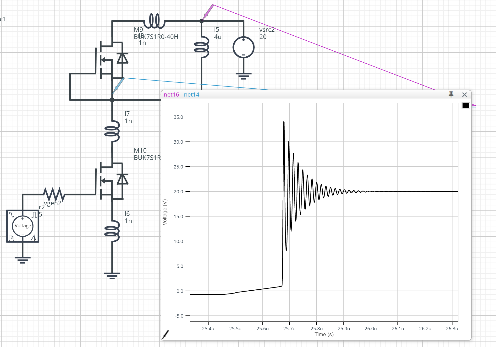
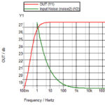
For this to be recognized in simulations, models must include the reverse recovery behaviour within the body diode, especially related to the frequency and damping of the resulting oscillations (ringing). Most simulation models provided by device manufacturers omit this information. Therefore, the amplitude of the ringing caused at the second switch-on can seem significant. As shown in Figure 1, a double-pulse simulation using a set of standard MOSFET models indicates a voltage overshoot of 75% with a duration of approximately 500 ns.
However, practical evaluation of actual devices in a laboratory environment shows that this level of ringing does not occur in the real world. This is due to the standard model not capturing the reverse recovery behaviour of the body diode. This is an issue for the circuit designer as the simulated ringing is large enough to mask other important effects relating to the presence of other parasitic effects. Unfortunately, it is likely that these issues will only be seen once a board has been constructed.
The omissions within manufacturer models preclude their use in gauging the EMC performance of a circuit. EMC can only be assessed following detailed laboratory testing, which occurs later in the product development process. At this point, design changes – such as those to improve EMC performance – are more time-consuming and expensive.
New advanced electrothermal models
Understanding the shortcomings of manufacturer-supplied MOSFET models, Nexperia developed advanced electrothermal models suitable for use with tools such as SPICE and VHDL-AMS. The goal was models that more accurately capture the behaviour of Nexperia power MOSFET devices – including an accurate representation of the reverse recovery operation of the body diode.
To demonstrate the improvement, Figure 2 shows the simulation of the same device (a BUK7S1R0-40H N-channel 40 V,1mΩ MOSFET in LFPAK88) as simulated previously, but this time based upon the new electrothermal models. Significantly less ringing is present, and the duration is less than half (now under 200 ns) than indicated by simulations based on the standard models.
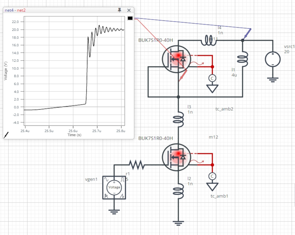
With the extra parametric information they include, the new models can create simulations that differ from real-world results by less than 1% for certain parameters. With this level of accuracy, designers can be confident that simulated results for EMC will be very close to the actual results obtained in the laboratory with real hardware.
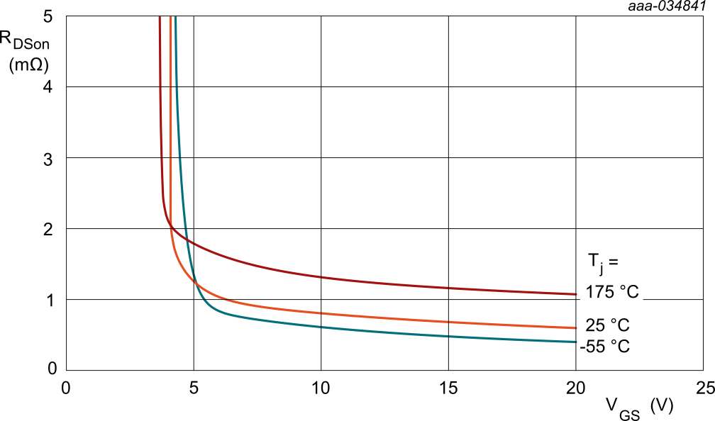
Additionally, the new models are accurate across the full operating temperature range of devices, not just at a nominal value. By way of example, Figure 3 shows the results from a simulation of on-resistance (RDS-ON) for Nexperia MOSFETs right across their operating temperature range of -55°C to 175°C. In fact, the new models are flexible enough to perform simulations at any required temperature, allowing designers to have a high degree of confidence in how designs will perform in the end application before committing to hardware.
Summary
While MOSFET models provided by many manufacturers are somewhat useful, they often omit key parameters that allow critical performance aspects such as EMC to be modelled accurately.
However, new advanced electrothermal models such as those provided by Nexperia include data to accurately model the reverse recovery performance of the body diode within their MOSFETs. This, along with the ability to simulate at any operating temperature, is a significant step forward – not least because accuracies exceed 99% on many parameters.
The new models overcome limitations in standard models that can often ‘mask’ phenomena that are not seen until the hardware is evaluated in the laboratory – leading to design more expensive changes or a design that is over-specified and not cost competitive.
With the new advanced electrothermal models, designers can have justifiable confidence in their designs much earlier in the design process.


Leave a Reply