
by Michael A. de Rooij, VP, Applications Engineering, Efficient Power Conversion
Though there are two standards for charging appliances wirelessly, a single circuit can be devised to serve as a charging node for both of them.
The good news about wireless charging techniques is that they do away with messy wiring that tethers phones and other appliances to wall outlets. The bad news is that there are multiple wireless charging schemes and they are generally incompatible with each other. Clearly, this incompatibility is not part of the formula for widespread adoption of wireless power technology.
This is the reason why manufacturers are trying to come up with a multi-mode capable wireless power design. Such a design could handle the two main competing wireless technologies: inductive coupling (also known as Qi), adopted by the Wireless Power Consortium (WPC) along with the Power Matters Alliance (PMA), and the highly resonant method adopted by the Alliance for Wireless Power (A4WP). Recently PMA and A4WP merged to become known as AirFuel.
An amplifier that can operate to all the wireless power standards must be capable of operating at both high (6.78 MHz) and low (100 to 367 kHz) frequencies efficiently. A single amplifier design like this has been elusive, so multi-mode source solutions have resorted to using multiple amplifiers, each driving their own corresponding source coil. This approach has generally been expensive with limited market appeal.
However, there is a simple single-amplifier topology based on eGaN FETs that is capable of operating to all of the mobile device wireless power standards. The design is based on a modified ZVS (zero-voltage switching) class D amplifier topology coupled to a specially designed source coil. The system components have been individually experimentally verified to the A4WP class 2 and Qi/PMA standards and are designed to efficiently deliver up to 10 W.
Wireless power system overview
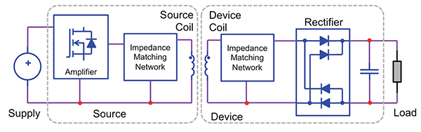
The general architecture of a wireless power transfer system generally consists of four basic building blocks: an amplifier, also known as a power converter; a source coil that includes a matching network; a device coil that includes a matching network; and a rectifier with high-frequency filtering. This architecture is similar regardless of inductive coupling or highly resonant wireless power technology.
It takes a thorough understanding of how the highly resonant coil and inductive coil systems operate to properly design the amplifier that can drive both modes efficiently. The complete schematic for a highly resonant wireless power coil system uses both shunt and series tuning in the device coil and only series tuning in the source coil. An equivalent circuit of a transformer represents the coupling between the two coils. This equivalent circuit is used to analyze the reflected impedance (labeled ZCoil_Tuned in the above diagram) presented at the source terminals as a result of varying load power. This reflected impedance would arise from a charging battery and manifests as a varying dc load resistance (labeled Rload in the diagram).
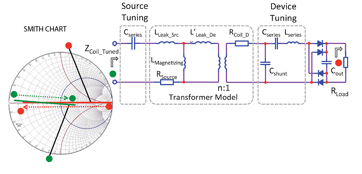
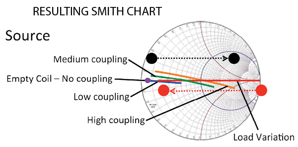
Starting with a high dc load resistance value (shown by the red dot a in the accompanying Smith chart and decreasing until it reaches red dot b), the reflected impedance of the tuned source coil is shown by the green trace and moves in the opposite direction starting with a low impedance at green dot a and increasing until the end at green dot b. This is the negative impedance effect of the highly resonant wireless power coil-set.
There is a similar analysis for the inductive coil set. The device and source coils are still tuned, but at different operating frequencies and for different reasons. Here, the tuning is used to set a specific inductance for the reflected coil impedance that is used by the amplifier for optimal operation.
The coupling between the source coil and device coil will also affect the reflected impedance and must be considered in the design, particularly for the highly resonant operating mode. The reason will become apparent once the inductive system coil is integrated with the resonant coil and their effects must be analyzed in unison.
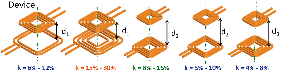
The coupling between the two coils is affected by changes in the distance and the turns ratio between them. If one assumes a fixed dc load resistance variation, then changes in distance between the coils, represented by d1, d2 and d3 in the figure below, show that as the coils get farther apart, the reflected impedance variation drops. For a fixed number of turns and a fixed turns ratio between the coils, this can be a bad outcome. It can be corrected by changing the number of turns on the source coil, where reducing the number of turns will reduce the reflected impedance range. The source coil is adjusted for compatibility with existing devices and the charging coils they contain.
In a multi-mode system, the ability to custom design the coil is critical to finding the optimal operating points for both the coil set and amplifier, as well as for realizing high system efficiency. Charging systems based on inductive coupling typically demand good coupling between the device and the source. Consequently, the distance between the coils is kept fairly short.
In the case of charging systems based on highly resonant methods, the coils typically sit further apart with more spatial freedom. It is important to artificially reduce the coupling between the coils so as to re-align the reflected impedance of the source coil to the optimal operating point of the amplifier. One way to accomplish this is to reduce the number of turns on the source coil.
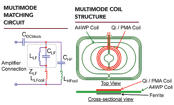
The coil set design is only the first step toward realizing a single amplifier operating multi-mode. The source coil must be assembled so it can be driven by a single amplifier. The figure to the left shows the top view and cross-section of such an integrated coil structure. Coil selectivity is implemented by changing the frequency of operation using applicable matching circuits. There is inherent coupling between the coils in the integrated structure that usually forces designs to incorporate decoupling circuitry between the inductive mode and highly resonant mode coils. This decoupling can be realized using a parallel resonant circuit (LLF and CLF) as depicted in the figure below. The circuit effectively blocks high frequency current. At low frequencies, the highly resonant tuning capacitor (CHF) blocks current.
A multi-mode amplifier topology
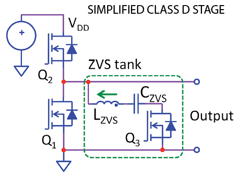
A single amplifier can now be used to drive the integrated coil structure. The ZVS class D amplifier has proven to be a simple high-efficiency solution for 6.78-MHz highly resonant wireless power applications. The circuit that establishes ZVS for high-frequency operation must be disconnected to let the amplifier operate at low frequency in hard-switching mode without leading to over-current.
In the case of the low-frequency system, hard-switching operation was still able to yield amplifier efficiencies well above 90%. Using the ZVS technique for the amplifier, amplifier efficiencies exceeding 85% could be realized for most operating conditions when operating at 6.78 MHz.
eGaN FETs have proven to be efficient in the range of 100 to 367 kHz, despite operating in hard-switching mode. This is because of their lower input capacitance (CISS), output capacitance (COSS), excellent Miller ratio (QGD/QGS1, and lack of reverse recovery (QRR). The figure below shows a multi-mode amplifier employing eGaN FETs. A small low-cost eGaN FET (Q3) disconnects the ZVS tank circuit from the amplifier to let it operate in hard-switching mode. This device can be driven directly from logic as it does not switch at high frequency. A suitable device for this application is the EPC2036.
The eGaN FET ZVS class D amplifier has been tested to both the A4WP class 2 (at 6.78 MHz) and Qi-A29 (at 130 kHz) standards independently. The A4WP system used the NuCurrent class 2 coil that was paired with a category 3 device and powered by an EPC9510 amplifier. The Qi system used a Würth coil set powered by a modified EPC9509 amplifier.
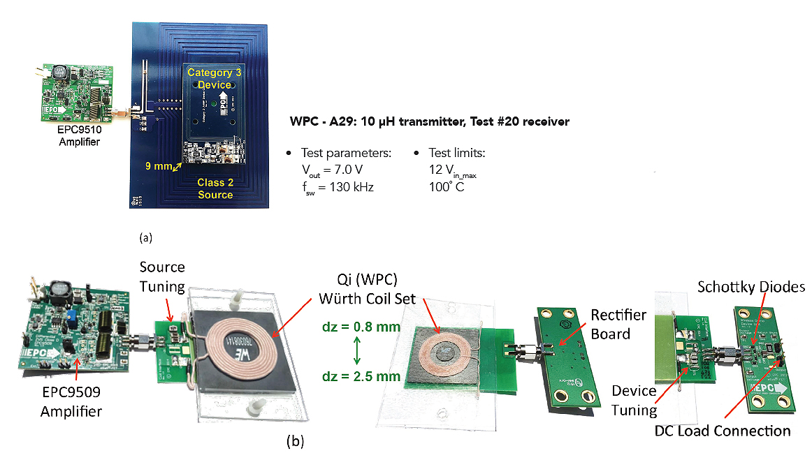
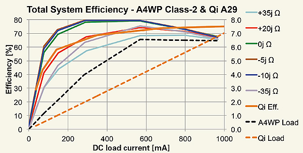
Tests show the A4WP test platform fully complies with the A4WP class 2 standard. The experimental evaluation used two different amplifier boards. To keep costs down, a single-ended amplifier was used for the highly resonant case. For the inductive system, the WPC (Qi) standard required a full bridge amplifier. Ultimately, a single-ended half-bridge configuration would be adopted for the final multi-mode amplifier as the coil design and tuning would be optimized for both high- and low-frequency operation.
References
For more on inductive coupling: “System Description Wireless Power Transfer,” Vol. I: Low Power. Part 1: Interface Definition, Version 1.2, June 2015.
Power Matters Alliance. [Online] Available: www.powermatters.org
For more on highly resonant charging: A4WP Wireless Power Transfer System Baseline System Specification (BSS), A4WP-S-0001 v1.3.1, February 25, 2015.
For more on coil matching circuits: V. Muratov, “Multi-Mode Wireless Power Systems can be a Bridge to the Promised Land of Universal Contactless Charging,” Wireless Power Summit, Berkeley CA, U.S.A., November 2014.
For more on ZVS class D amplifiers: M. A. de Rooij, “Performance Comparison for A4WP Class-3 Wireless Power Compliance between eGaN FET and MOSFET in a ZVS Class D Amplifier,” International Exhibition and Conference for Power Electronics, Intelligent Motion, Renewable Energy and Energy Management (PCIM – Europe), May 2015.
M. A. de Rooij, “Wireless Power Handbook,” Second Edition, El Segundo, October 2015, ISBN 978-0-9966492-1-6.
A. Lidow, J. Strydom, M. de Rooij, D. Reusch, “GaN Transistors for Efficient Power Conversion,” Second Edition, Wiley, ISBN 978-1-118-84476-2.
For more on GaN transistors and the EPC2036 in particular: D. Reusch, J. Strydom, and A. Lidow, “Highly Efficient Gallium Nitride Transistors Designed for High Power Density and High Output Current DC-DC Converters,” IEEE International Power Electronics and Application Conference (PEAC), pp.456-461, 2014.
Efficient Power Conversion, “EPC2036—Enhancement Mode Power Transistor,” EPC2036 data sheet, April 2015, [Online] Available: www.epc-co.com/epc/Products/eGaNFETs/EPC2036.aspx
For more information on charging coils: NuCurrent. coil part number PNC21-T28L04E-152991R40, www.nucurrent.com
Würth Elektronik “WE-WPCC Wireless Power Charging Transmitter Coil,” 760308141 data sheet [Online] Available: www.katalog.we-online.com/pbs/datasheet/760308141.pdf
Würth Elektronik “WE-WPCC Wireless Power Charging Receiver Coil,” 760308102210 data sheet [Online] Available: www.katalog.we-online.com/pbs/datasheet/760308102210.pdf
Leave a Reply