
Smart use of protection components can help give consumers a trouble-free charge.
Todd Phillips Littelfuse Inc.
The convenience that wireless charging systems provide has made them increasingly popular for use with consumer goods and appliances. But the development of wireless charging devices creates a number of challenges for designers. Most wireless applications are characterized by limited space for circuitry and cost considerations. So designers must minimize component counts without compromising quality.
Simultaneously, designs must also protect against failures related to overloads and transients. And energy efficiency is usually a priority as well. Also, products must comply with international standards for safety, surge and transient protection. Thus it is useful to understand the methods available for protection, efficient control, and safety sensing of wireless chargers.
A wireless charging system consists of three elements; a power adapter, a charging cable, and a charging pad. The power adapter converts the ac voltage from the power line into a dc voltage. The charging cable sends power from the power adapter to the wireless charging pad. The charging pad then transmits power wirelessly to the device-to be-charged.
The power adapter must contend with any overload and transient conditions presented by the ac mains. Circuit protection generally is at the input stage. Common electrical hazards include; induced lightning voltage surges, switching surges, electrostatic discharge, and overload fault currents. Low-power power adapters use a variety of overvoltage protection schemes. MOVs are often the choice for power adapters where long-term reliability is a priority.

Fuses are the primary choice for overcurrent protection, especially for higher-power adapters. Designers have a wide range of options when deciding on the fuse form factor. The main choices are cartridge fuses, thru-hole fuses, or surface-mount fuses. Surface-mount fuses typically take up the least amount of PCB real estate.
Regardless of fuse form factor, the fuse must have voltage and current-interrupting ratings sufficient to do the job. Designers frequently consider a time-lag fuses to avoid nuisance tripping from overvoltage events. Each fuse type responds differently to overloads. In addition, designers trying to maximize energy efficiency should evaluate the fuse watts-loss rating.
Designers can maximize charger efficiency by selecting MOSFETs with low on-state resistance, low gate charge, and a high dv/dt rating to reduce switching loss and obtain faster switch transition times. MOSFETs with low on-state resistance and high dv/dt parameters can switch at higher frequencies, enabling a more efficient switch-mode supply circuit topology. For the same reasons, designers should use MOSFETs with internal soft-recovery diodes which reduce turn-off transients and reduce electromagnetic emissions (EMI).
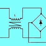
In many supply topologies, a step-down transformer reduces an ac voltage and Schottky diodes then rectify the signal back to dc. Schottky diodes with low forward-voltage-drop and which can operate at high frequencies are suggested for this section of the design.
Transient voltages on the input of the supply can find
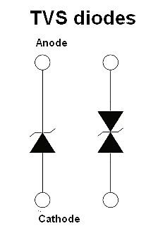
their way to the output rectifiers. Some of these transients may be large enough to damage the power-semiconductor devices. Transient voltage suppression (TVS) diodes can provide a level of protection. TVS diodes can respond to a transient extremely quickly, typically in under one picosecond. They also have low clamping voltages to protect sensitive electronic circuits. Designers can select either uni-directional or bi-directional configurations of a TVS diode.
The USB Type-C protocol allows up to 100 W of charging to speed the re-charging process. This is a substantial increase in available power over earlier USB standards. This high-level power protocol uses USB Type-C connectors which have a 0.5-mm pitch, five times smaller than USB Type-A connectors.
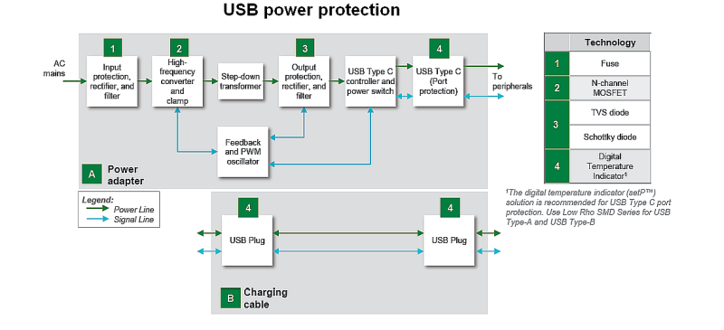
The application of more power in less space increases the risk that dust and dirt will create a resistive fault between pins on the connector and create a hot spot. Designers should consider using a digital temperature indicator, like the PolySwitch setP, to detect over-temperatures. The setP temperature indicator measures less than a tenth-of-an-inch square and exhibits a rapid rise in resistance as temperatures increase from about 80 to 100°C. It is designed to be used in the Configuration Channel (CC) line of the Type-C connector to detect over-temperature events and help protect the circuit.
The setP temperature indicator complies with the USB Type-C standard for monitoring the temperature of USB Type-C connectors. Details on the circuit configuration for this protection scheme are in the USB Type-C cable and connector specification.
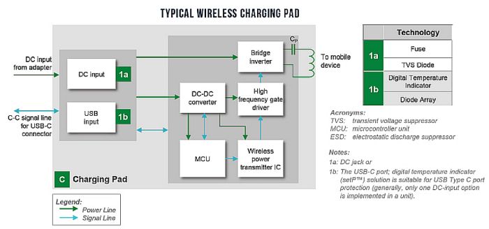
Protecting the wireless charging pad
Power for the wireless charging pad comes from either a proprietary dc input or a USB port. Designers should protect the dc input circuit from both overloads and transients. Regardless of the type of power input used, protection is highly recommended.

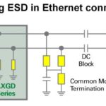
On the dc input circuit, designers should consider overload protection via fast-acting fuses. Small surface-mount fuses rated for the proper dc voltage are suited for this purpose. For transient protection, surface-mount TVS diodes are available which can provide up to ± 30 kV of ESD protection and 1,500 W of peak transient power absorption. Low clamping voltages, common for most TVS diodes, help avoid stressing downstream circuit components when a transient strikes.
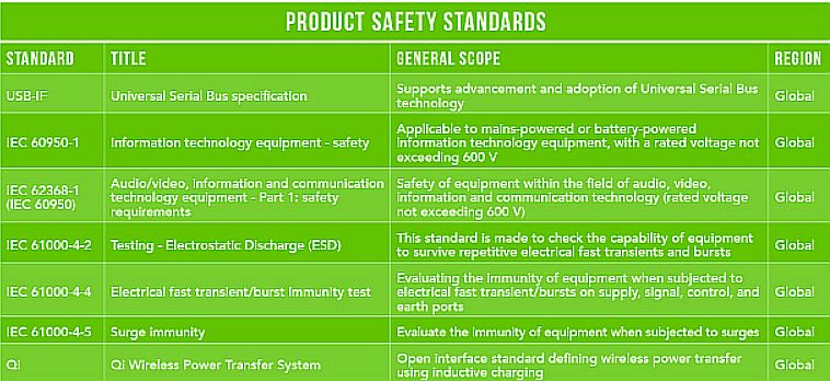
Of course, wireless chargers must comply with international standards. The standards define minimum safety requirements and spell out tests that evaluate various electrical hazards such as ESD, electrical fast-transients, and surge levels. Wireless chargers using USB communication must ensure interoperability according to the Universal Serial Bus (USB) standard. Designers should also be familiar with the Qi wireless charging protocol that defines how energy transfers to product batteries.
Circuit protection can help ensure a positive end-user experience. In that regard, manufacturers of protection components can make available application engineers early in the design cycle who can save substantial development time and reduce design revisions.
References
Littelfuse Circuit Protection Selection Guide
Littelfuse PolySwitch setP Design Guide

I appreciate the research and detail put into explaining all the various places one can introduce protection mechanisms on the supply side of the circuit.
I had never heard of setP before though so that was especially interesting.
I’m curious though – I see in the transmitter pad there are multiple ‘intelligent’ components including the MCU and transmitter IC. How does the transmitter detect an object in the electrical field though? Is this a function of the receiver? Or is it protocol-dependent?
Again, I was just wondering how modern charging protocols maintain safety when resonance with objects – especially metal – in an inductive field can become dangerous.