SiC FETs now include measures aimed at keeping losses down while managing fast switching waveforms.
Dr. Anup Bhalla | UnitedSiC
Silicon carbide (SiC) FETs have low on-resistances, fast switching speeds, and intrinsic diodes with low reverse recovery charge (QRR) and low forward-drop (VF) qualities. These qualities make SiC FETs suitable for use in active-front-end three-phase rectifiers, totem-pole power-factor correction (PFC) stages, interleaved PFC circuits, phase-shift full bridges, LLC and dual active-bridge circuits.
To get the best from these devices, it is important to understand how system layout, thermal, power density and EMI constraints affect their performance.
UnitedSIC’s SiC FETs are cascoded devices formed by co-packaging a silicon MOSFET and a SiC JFET. It is useful to briefly explore what the cascode structure brings to SiC components. As a quick review, a cascoded JFET and MOSFET consists of a low-voltage MOSFET with its drain connected to the source of the JFET. The JFET gate is connected to the MOSFET source. The input to the cascoded combination is the gate of the MOSFET; the drain is the JFET drain, and the source is the MOSFET source.
A JFET is normally on, and the MOSFET is normally off. The JFET VGS is the inverse of the MOSFET VDS. The more positive the MOSFET VDS, the more negative the JFET VGS. When the MOSFET is off (VDS rises), the JFET turns off.
The conventional view of SiC JFETs is that their non-standard drive voltages and lack of an intrinsic diode makes them difficult to work with. The use of a JFET in cascode with a MOSFET solves both of these issues. It uses the MOSFET’s intrinsic diode while switching inductive loads and can be driven using low-voltage MOSFET drive voltages. Additionally, a JFET cascode actually performs better than a SiC MOSFET alone over temperature and at higher values of di/dt.
UnitedSiC SiC FETs have a low specific on-resistance and sit in a thermally enhanced standard package. The devices are offered in two speed classes which are set during manufacturing by adjusting the gate resistance of the SiC JFET.
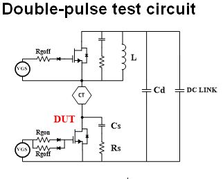
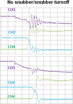
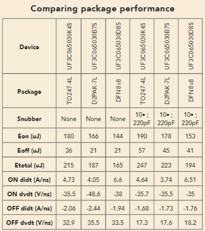
The UJ3C series switches more slowly and has the higher QRR but is easier to use in standard three-leaded packages. In contrast, the UF3C devices are about twice as fast as the UJ3C parts and come in both three-leaded and Kelvin-source packages. These devices require a more careful circuit layout and benefit from the use of RC snubbers, especially for three-leaded packages with high common-source inductances.
The TO247-4L package adds a Kelvin-source connection to a standard TO247-3L. This feature enables users to overcome the limitations imposed by common-source inductances. It also enables faster switching speeds and higher di/dt, creating clean gate waveforms and avoiding false triggering. However, the loop inductance of half-bridge configurations
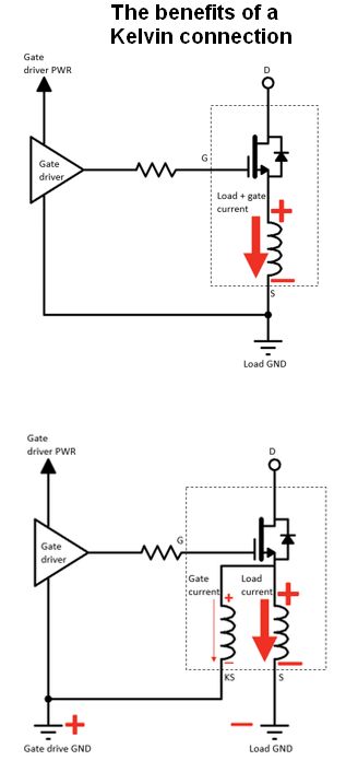
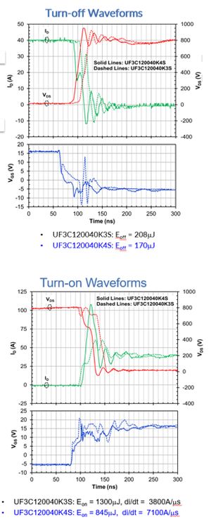
implemented in these packages stays quite high, in the 20-30 nH range, and this inductance leads to high voltage overshoots. These can be reduced using small RC snubbers.
The surface-mount D2PAK-7L package has much lower package inductance and half-bridge loop inductance than the three-leaded packages. The DFN8X8 package further reduces loop inductances, by up to 8 nH.
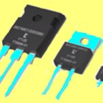
One reason that UnitedSiC can build high-performance cascode structures is that its SiC JFETs have drain-source capacitance (CDS) values that are almost zero. This low value prevents a capacitive voltage divider from forming between the low-voltage MOSFET and the SiC FET.
The low-voltage MOSFET is optimized for a ±25-V VGS(MAX) and a 5-V threshold voltage (Vth). This means that while its gate need only be driven from 0 to 12 V, it can also be driven across a wide range of operating voltages. Moreover, there is a relative absence of threshold-voltage hysteresis and negative gate-source voltage instabilities compared to conventional SiC MOSFETs. These properties make it possible to use the cascoded SiC FET at the same gate-drive voltages as superjunction MOSFETs, IGBTs or SiC MOSFETs, with large safety margins.
Cascode devices are built so the gate resistance (Rg) of the MOSFET slows the device’s VDS swing. VDS, in turn, acts as the VGS drive for the normally-on JFET, enabling some control of dv/dt and di/dt rates. The UJ3C series supports moderate dv/dt rates of 20-40 V/nsec, while the UF3C series covers the 40-100-V/nsec range.
The switching speed of SiC FETs enables faster turn-on and turn-off, and in the cascode configuration it also improves the Qrr.
The normally-on SiC FET technology used in these devices has a low specific on-resistance (RdsA). This low resistance makes possible small chip sizes, which reduce the output capacitance (COSS) values. Consequently, RC snubbers can have a relatively small value for CSNUB and are typically built using surface-mount components in parallel with the source and drain of the FET.
In practice, the need to simplify heatsinking may result in layouts with a significant total loop inductance. It may also be difficult to minimize the size of gate-drive loops, depending on the overall converter’s shape and size.
Small RC snubbers can effectively manage switching issues with fast SiC transistors. The use of a 220-pF, 10-Ω snubber can dramatically reduce voltage/current ringing. This reduction, in turn, improves the VGS waveforms, because most of the noise on the gate waveforms stems from the ringing current acting on the internal common-source inductance (which is large in the TO220-3L and TO247-3L packages).
At high currents, it’s possible to increase the rate at which current changes during turn-on by boosting the gate voltage drive from 12 to 15-20 V. Switching waveforms are also well controlled in the presence of a similar snubber.
Pushing to higher speeds
While it is less common to produce SiC MOSFETs in Kelvin-source packages, their performance benefits make them increasingly attractive. A Kelvin connection puts the common-source inductance outside the gate drive loop. Consequently, the Kelvin-source connection bypasses any voltage drops developed across this inductance during rapid changes in current flow. Those voltage drops slow the device turn-on and turn-off.
It is important to use isolated gate drivers with such Kelvin-source packages, because the return for the gate is no longer at the same voltage as the power source. The gate-drive power rails must therefore also be isolated, or the gate driver must be able to withstand some voltage bounce between the source and the Kelvin-source connections.
If circuits are to be driven by a control IC with built-in drivers, designers must ensure the IC can only see the differential voltage across the external current-sensing resistor that is in series with the Kelvin-source device.





Leave a Reply