
Here’s how to evaluate energy efficiency associated with components that make up widely used power conversion circuitry.
FRANK DE STASI, MATHEW JACOB, TEXAS INSTRUMENTS INC.
IN SOME WAYS, selecting a module, converter or controller for power conversion resembles deciding whether to take a flight, board a train, or drive from point A to B. Once you’ve decided an airplane is your mode of transportation, for example, it’s easy to pick an airline to fly.
 Let’s start with the definition of each device type:
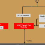
A controller can be used with external field-effect transistors (FETs), inductors and capacitors.
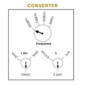
A converter is a controller plus integrated FETs that uses external inductors and capacitors.
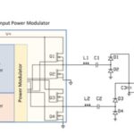
A module integrates both the FETs and the inductor but uses external capacitors.
It’s clear that with the progression of integration from controllers to modules, the main heat dissipaters (FETs, inductor) are brought in from the outside. The obvious advantage with integration is smaller size and ease of use. The clear disadvantage is the thermal challenge; you’ll need to optimize the devices to handle the thermals and still operate at a high ambient temperature.
Because thermals are directly related to power loss – which translates to efficiency – we’ll focus on efficiency improvement methodologies, or “knobs,” for each device option: modules, converters and controllers. As you progress toward more integration, there are fewer knobs available to optimize efficiency. That’s because converter and module manufacturers try to optimize the internals for efficiency over a wide range of operating conditions.
Realistically, the knobs on a controller will be numerous because the internal parameters of the FET constitute knobs that affect switching losses. It is possible to get much better efficiency with similar on-resistance (or RDS[on]) FETs if the other internal parameters of the FET that affect switching losses are lower. In general, the lower the capacitance or charges inside the FET, the less the loss.
The most widely used knobs for converters generally include the operation frequency, the switching FET Rdson_HS and Rdson_LS, and the inductance value and series resistance of the coil used to store switching energy. Now we’ll examine each of these knobs in detail and see how they affect efficiency. Each knob affects losses, so start with the loss equation for a buck topology (Pcond and PSW):

Here, D = The switch duty cycle of converter. This is the proportion of the total period that the high-side MOSFET is on; FSW = Converter switching frequency = 1/period; IO = Load current of the dc/dc converter; L = Inductance value of power inductor, h; PCOND= Conduction losses of the system. These losses are due to current flowing in resistances; PCORE = Power loss due to eddy currents and hysteresis in the core of the power inductor; PCOSS = Power loss due to the capacitance of the power MOSFETs, W; PSW = Switching losses. These losses are due to the switching nature of the dc/dc converter and are usually proportional to FSW; QG = Gate charge required to turn on the power MOSFETs; RHS = Resistance of high-side MOSFET (RDSON), Ω; RL = Resistance of the power inductor, Ω; RLS = Resistance of low-side MOSFET (RDSON) , Ω; Tt = Transition time of the switch waveform, sec.; VG = Gate drive voltage for the power MOSFETs, V; VIN = Input voltage to the converter, V; VOUT = Output voltage of the converter, V; and ΔI = Peak-to-peak magnitude of the inductor ripple current.

The losses are split into two groups: Pcond and PSW. The total loss is the sum of the two. Pcond represents the conduction losses from current flowing in the various resistances. For a buck converter, this current is Io, the output current.
Notice that the conduction loss is proportional to the square of the output current. This loss can grow large for higher-load-current applications. Both the MOSFET and inductor contribute resistances to the converter.
In the previous PCOND equation, the term within the square brackets represents the effect of the ripple current in the inductor, ΔI. Because the inductor current contains both dc and ac components, this term accounts for the rise in root-mean-square (RMS) current flowing through the loss-producing resistances. The value of ΔI depends both on the inductor and the switching frequency.
It’s the nature of a dc/dc converter that causes switching losses in a buck regulator. A rectangular waveform appears on the switch node of the regulator. This signal switches from near-zero volts to near VIN, with fast transition times. Because the inductor will hold the current constant during these transitions, there will be an overlap between current and voltage, and therefore a power loss.
The first term in the previous PSW equation accounts for this loss, with Tt equal to the rise and fall time of the switch waveform. The loss is also proportional to the input voltage and load current. The MOSFETs must switch on and off at the switching frequency rate, which requires some energy from the gate driver supply.
This gate drive loss is represented by the second term in the previous PSW equation. It depends on the value of the gate driver supply voltage, VG, and the total gate charge for both MOSFETs, QG. PCORE is the core loss of the inductor. Because the inductor has an ac component of current flowing through it, there will be an ac component of core flux. This will cause power loss in the core due to hysteresis and eddy
current effects.
All of the terms in the previous PSW equation are proportional to the switching frequency, except Pcore. Pcore will usually depend on switching frequency to a higher power than one. The total power loss is then the sum of Pcond and PSW.
Frequency
Recall that the switching frequency comes into the total loss equation in the switching-loss terms and sets the inductor current ripple along with the inductor value. From the
PSW equation, it’s clear that a higher frequency will create more switching losses. These losses arise both in the MOSFET and in the core of the inductor.
You may think that use of the lowest switching frequency would offer the best efficiency. This would be true if the inductor size did not depend on the switching frequency. As will become clear, the trade-off between inductor size and switching frequency is important.
The power inductor is a key component in any dc/dc converter. In conjunction with the output capacitor, the inductor smooths the rectangular waveform at the switch node and provides the regulator’s dc output. The inductor is sized based on the desired ripple current, ΔI, using the equation:
It’s typical practice to select a ripple current of about 30 to 40% of the converter’s full-load current. From the above equation, there’s an inverse relationship between switching frequency and inductor value. This implies you can reduce the switching frequency to improve efficiency and choose a larger inductor value to keep the same ripple current.
Unfortunately, there are several trade-offs that get in the way.
First, a larger inductor value means a physically larger inductor, occupying more printed circuit board (PCB) area. More important, a larger inductor value will require more turns on the core. More wire in the inductor means more dc resistance for a given physical size. The higher dc resistance will produce more losses and lower the efficiency. The RL term in the PCOND equation models this effect.
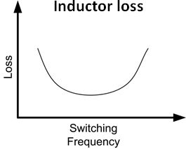
There will usually be an optimum switching frequency that will provide the lowest losses. As you change the frequency, you adjust the size of the inductor to keep the same ΔI. At high frequencies, the switching losses will rise; at low frequencies, the inductor will get larger and produce more losses from dc resistance.
The core losses of the inductor will also depend on switching frequency, sometimes in a complex way, but always rising with frequency. The type of core material plays a large role in core losses. Typically, a powdered-iron core will have more loss at switching frequencies greater than about 1 MHz compared to a ferrite-type core. The best way to estimate inductor core loss is to use the graphs or calculators on the inductor manufacturer’s website.
Careful choice of the switching frequency and inductor will go a long way toward minimizing overall losses. Setting the switching losses equal to the conduction losses is a widely used approach that provides good results in the majority of cases.
MOSFETs
With a controller, designers must choose the power MOSFETs as well. Depending on the type of controller, at least one high-side FET and perhaps one low-side FET are necessary. In a dc/dc converter, the power FETs serve as switches. In a controller, the
parameters important for efficiency are the RDS(on) and the charges required to turn the FETs on and off at the switching frequency.
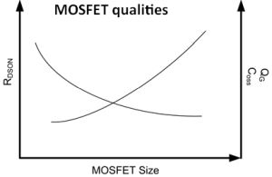
In the PSW equation, these terms are represented as RHS, RLS, QG and Pcoss. The Pcoss term represents the loss when charging and discharging the drain-to-source capacitance of the FETs. The conduction losses from the MOSFETs also depend on the steady-state duty cycles, D and 1-D. It would seem intuitive, then, to choose FETs with the lowest RDS(on) and lowest QG and Pcoss. Unfortunately, the RDS(on) and FET charge parameters are inversely related.
As the size of the MOSFET grows, the RDS(on) and conduction loss will diminish. However, the gate charge, drain-to-source capacitance, and switching losses will rise. So, again, you will need to trade off RDS(on) and switching losses to minimize overall loss.
As with the inductor selection, try to choose a MOSFET so the switching losses equal conduction losses. That method also works well when selecting the relative sizes between the high-side and low-side FETs; size them so the MOSFET conduction losses are equal. From the PCOND equation, you can derive:
Because you know the operating duty cycle, you can choose either the high- or low-side FET and determine the size of the other.
Having looked at the various knobs available to optimize efficiency or reduce losses in a buck dc/dc stage, it’s clear there is a lot more leeway to optimize a controller design. It’s a big plus to have control of the FET and inductor sizing.
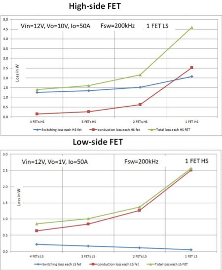
There are some instances where use of parallel FETs in controller design help keep the power dissipation in each FET under control. A rule of thumb is that anytime you use FETs in parallel, losses rise. Even if you reduce the conduction losses, the rise in switching losses dominate, and the total losses go up. Switching losses rise because of the added capacitance when connecting FETs in parallel. However, the ability to distribute the loss across multiple FETs helps limit the temperature rise in each FET.
In a nutshell, there are various knobs available for designers when choosing a power-conversion device. The knobs specifically affect efficiency. Whether you choose a controller, a converter or a module, a little care in the selection of switching frequency, inductor and MOSFET can ensure that your design is optimally efficient and with minimal temperature rise.


Leave a Reply