
by Alex Lidow, CEO, Efficient Power Conversion Corp.
It can be tricky to analyze power supply designs incorporating GaN power devices. Here are the basics of calculating losses and device currents when using these exotic semiconductors.
There is a lot of activity in wide-bandgap semiconductors these days. They have the ability to operate at much higher voltages, frequencies and temperatures than conventional semiconductor materials. Power circuits built around wide-bandgap devices can be cheaper and more energy efficient than their silicon counterparts.
One type of wide-bandgap technology for making power transistors uses gallium nitride grown on top of silicon. Enhancement-mode transistors, such as eGaN FETs from EPC, have qualities resembling those of power MOSFETs but with better high-speed switching, lower on-resistance, and a smaller size than their silicon predecessors.
But eGaN transistors aren’t one-for-one replacements for silicon MOSFETs. Nor can eGaN power supply circuits be analyzed in exactly the same way as those created with MOSFETs.
In that regard, we recently ran an informal online contest that asked contestants to solve ten story problems centered on power supply design with eGaN devices. Winners received a copy of the hardcover textbook, GaN Transistors for Efficient Power Conversion, 2nd Edition.
The problems in our challenge proved to be difficult for most people. Only a handful of entrants got a perfect score and earned a copy of the book.
In the interest of promoting power supply education, here are the questions and the solutions that eluded a majority of contest entrants. Engineers engaged in cutting-edge power design would be well served by spending time understanding the concepts behind the answers.
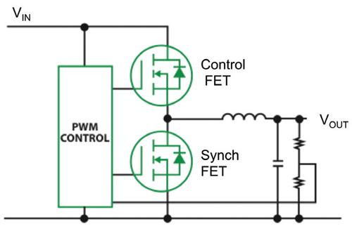


Q1: Consider the buck converter circuit in the accompanying diagram, the switch-mode waveform, and eGaN and conventional MOSFET body diode operating curves provided here. In the buck converter, assume
VIN = 12 V, VOUT = 1.2 V, IOUT= 20 A, and fSW = 200 kHz. Td(on) = Td(off) = 20 ns.
Calculate both the MOSFET and eGaN FET body diode power loss. They are both operating at room temperature (25 C).
ANSWER:
The power loss in the body diode is the product of the frequency, output current, and the voltage drop across the body diode (Vsd) multiplied by the amount of time the diode is conducting. Given fsw = 200 kHz., Td(on)+Td(off) = 40 ns; Pdiode = (Td(on) + Td(off)) x fsw x Iout x Vsd
For the MOSFET, Vsd = 0.7 V at 20 A and 25ºC;
Pdiode(MOSFET) = 40 ns * 200 kHz * 20 A * 0.7 V = 0.112 W.
For the eGaN FET, Vsd =2 V at 20 A and 25ºC;
Pdiode(eGaN) = 40 ns * 200 kHz * 20 A * 2 V = 0.32 W.
Q2: In the same buck converter,
VIN = 12 V, VOUT = 1.2 V, IOUT = 20 A, fsw = 1 MHz.. If the Td(on) = Td(off) = 20 ns,
Calculate both the eGaN FET and MOSFET body diode power loss. Again, both operate at room temperature (25 C).
ANSWER:
The power loss in the body diode is the product of the frequency, output current, and the voltage drop across the body diode (Vsd) times the amount of time the diode is conducting. Recall fsw = 1MHz, Td(on) + Td(off) = 40 ns.
For the MOSFET, Vsd = 0.7 V at 20 A and 25ºC from the supplied curve.
Then Pdiode(MOSFET) = 40 ns * 1 MHz * 20 A * 0.7 V = 0.56 W.
From the supplied curve for the eGaN FET, Vsd = 2 V at 20 A and 25ºC.
Pdiode(eGaN) = 40 ns * 1 MHz * 20 A * 2 V = 1.6 W.
Q3: Same buck converter.
VIN = 12 V, VOUT = 1.2 V, IOUT = 20 A, fsw = 1 MHz. If the Td(on) = Td(off) = 2.5 ns,
Calculate both the eGaN FET and MOSFET body diode power loss. We’re still at 25ºC.
ANSWER:
The power loss in the body diode is the product of the frequency, output current, and the voltage drop across the body diode (Vsd) times the amount of time the diode is conducting. Thus Td(on)+Td(off) = 5 ns. For the MOSFET, Vsd = 0.7 V at 20 A and 25ºC.
Pdiode(MOSFET) = 5 ns * 1MHz * 20 A * 0.7 V = 0.07 W.
For the eGaN FET, Vsd = 2 V at 20 A and 25ºC.
Then Pdiode(eGaN) = 40 ns * 1MHz * 20 A * 2 V = 0.2 W.

Q4: Same buck converter.
VIN = 12 V, VOUT = 1.2 V, IOUT = 20 A, fsw = 200 kHz.
Calculate the inductor and capacitor values needed to achieve a ripple current (dIL) of 5 A and an output ripple voltage (dVpp) of 50 mV. (Hint: Remember from the inductor law, VL = L di/dt. The duty cycle of the buck converter is given as D = VOUT/VIN.)
ANSWER:
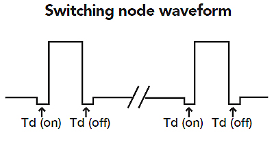
For questions four and five, refer to the diagram of the buck converter output waveform. Solving the inductor law relationship for L, L = VL / (di/dt).
For the capacitor, use dIL(RMS)/dt = Cmin * dVpp ; dIL/(8*fsw) = Cmin * dVpp . For 200 kHz, the ramp time for the inductor is: dt = 0.1/200 kHz = 0.5 μs; di = 5 A; VL = (12 V – 1.2 V); L= (10.8 V) /(5 A / 0.5 μs) = 1.08 μH;
Cmin = 5 A /(8 * 200 kHz * 50 mV) = 62.5 μF
Q5: Same buck converter.
VIN = 12 V, VOUT = 1.2 V, IOUT = 20 A, fsw = 1MHz.
Calculate the inductor and capacitor values needed to achieve a ripple current (dIL) of 5 A and an output ripple voltage (dVpp) of 50 mV. (As in question four, remember from the inductor law, VL = L di/dt. The duty cycle of the buck converter is given as D = VOUT/VIN.)
ANSWER:
The calculation process proceeds similarly to that in question four, but here L= (10.8 V) /(5 A / 0.1 us) = 0.22 uH;
Cmin = 5 A /(8 * 1 MHz * 50 mV) = 12.5 μF.
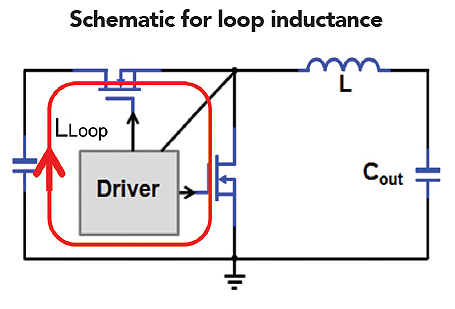
Q6: In the accompanying diagram of the buck converter,
VIN = 12 V, VOUT = 1.2 V, IOUT = 25 A.
How much is the power loss reduced if the loop inductance is reduced from 1.5 nH to 0.5 nH? fsw =1 MHz, L = 0.33 μH (Hint: To calculate the peak current, it might be helpful to remember that V = Ldi/dt.)
ANSWER:
Calculate the peak current from the relationship V = Ldi/dt; dt(on)=1.2 V/12 V x 1 MHz =0.1μs;
(12-1.2) V = 0.33 uH * (di/0.1 μs); di = 3.27 A; Peak current (Ipeak) = (di/2) + 25 A = 26.6 A; The energy saved in the loop inductance, E_LLoop = (1.5-0.5)/2 x Ipeak2 = 0.3538 J; The power saved in the loop inductance,
P_LLoop = 0.3538 * 1 MHz = 0.3538 W.
Q7: In the buck converter,
VIN = 12 V, VOUT = 1.2 V, IOUT = 25 A.
How much is the power loss reduced if the loop inductance is reduced from 1.5 nH to 0.5 nH? Fsw = 5 MHz, L = 0.1 μH (As in question six, to calculate the peak current, it might be helpful to remember that V = Ldi/dt.)
ANSWER:
Calculate the peak current by V = Ldi/dt;
dt(on) = 1.2 V/12 V x 5 MHz = 0.02 μs;
(12-1.2) V = 0.1 μH x (di/0.02 μs);
di = 2.16 A;
Peak current (Ipeak) = (di/2) + 25 A = 26.08 A;
Energy saved in the loop inductance, E_LLoop = (1.5 – 0.5)/2 x Ipeak2 = 0.34 J;
Power saved in the loop inductance,
P_LLoop = 0.34 x 5 MHz = 1.7 W.
Q8: For a 12-V input, 1.0-V output, 4-MHz 25-A buck converter, the designer wants to get the best performance and minimum loss on the low-side (Sync) FET. The controller has a minimum dead time of 25 ns. dIL = 4 A. Calculate the Sync FET losses assuming a BSZ0901NS. (Hint: From the BSZ0901NS data sheet, VDS = 30 V, RDS(on)max = 2.1 mΩ, ID=25 A. Qrr = 2 nC, VSD (30A) = 0.75 V, Freq = 4 MHz)
ANSWER:
The duty cycle D = 1/12 = 8.33 %; TON = 21 ns;
From the BSZ0901NS data sheet,
VDS = 30 V, RDS(on)max = 2.1 mΩ, ID = 25 A. Qrr = 2 nC, VSD (30A)= 0.75 V,
Freq = 4MHz. Cycle time = (1/4 MHz) T = 250 ns; TDeadtime = 2*25 ns = 50 ns;
Then sync FET conduction time Tsync = (250 ns – 21 ns – 50ns) = 179 ns.
Diode conduction losses during dead time = Vsd * Isd * tdeadtime * fSW;
Sync FET conduction losses = (IOUT2 + dIL2/12) x RDS(on) x Tsync/T.
The diode conduction losses are:
0.7 V x 25 A x 50 ns x 4 MHz = 3.5 W;
Sync FET Conduction Losses = 0.94 W;
Total = 4.44 W
Q9: For a 12-V input, 1.0-V output, 4-MHz 25-A buck converter, the designer wants to get the best performance and minimum loss on the low side (Sync) FET. The controller has a minimum dead time of 25 ns. dIL = 4 A. Calculate the Sync FET losses assuming a EPC2023.
(Hint: From the EPC2023 data sheet,
VDS = 30 V, RDS(on)max = 1.3 mΩ, ID =25 A. Qrr = 0.0 , VSD (30A)= 2.2 V, Freq = 4 MHz)
ANSWER:
From the EPC2023 data sheet,
VDS = 30 V, RDS(on)max = 1.3 m Ω, ID = 25 A, Qrr = 0.0, VSD(30A) = 2.2 V.
As in question eight, diode conduction losses are 2.2 V * 25 A * 50 ns * 4 MHz = 11 W; Sync FET conduction losses = 0.58 W;
Total = 11.58 W.
Thus the sync FET losses are substantially higher compared to a regular MOSFET with a fixed minimum dead time of 25 ns for the controller.
Q10: For a 12-V input, 1.0 V output, 4 MHz, 25-A buck converter, the designer wants to get the best performance and minimum loss on the low side (Sync) FET. The controller has a minimum dead time of 25 ns. dIL = 4 A. Calculate the Sync FET losses for a EPC2023 with a Schottky diode in parallel with a Vf = 0.4 V.
(Hint: From the EPC2023 data sheet,
VDS = 30 V, RDS(on)max = 1.3 m Ω, ID = 25 A, Qrr = 0.0, VSD(30A) = 2.2 V, cycle time = (1/4 MHz) T = 250 ns; TDeadtime = 2 x 25 ns = 50 ns.)
ANSWER:
The control FET duty cycle D = 1/12 = 8.33%; TON = 21 nS.
Sync FET conduction time = (250 ns – 21 ns – 50 ns) = Tsync = 179 ns.
Diode conduction losses during dead time = Vsd * Isd * tdeadtime x fSW = 2 W,
Sync FET conduction losses = (IOUT2 + dIL2/12) x RDS(on) x Tsync/T = 0.58 W. 2 + 0.58 = 2.58 W.
The sync FET losses drop substantially when a Schottky diode is used in parallel if the dead time is long (2 x 25 ns).
RESOURCES
GaN quiz on powerelectronictips.com,
www.powerelectronictips.com/pop-quiz-aceegan-fet-quiz-win-textbook-egan-uber-guru/
GaN Transistors for Efficient Power Conversion, 2nd Edition,
www.wiley.com/WileyCDA/WileyTitle/productCd-1118844769.html
Efficient Power Conversion Corp.,
http://epc-co.com/epc
[…] resources: “Power converters with GaN,” by Alex Lidow, CEO of […]