
Welcome to this Virtual Interview on power distribution network (PDN) integrity in embedded systems. We are here today with Heidi Barnes (HB), Senior Application Engineer for PathWave EDA for High Speed Digital with Keysight Technologies. The following is from an interview with Heidi by EEWorld’s Jeff Shepard where they discuss the use of decoupling capacitors and other considerations when minimizing potential noise problems as well as static and dynamic analysis of PDNs in embedded systems.
JS: Heidi, What are the important considerations when sizing and placing decoupling capacitors?
HB: Remembering that they come with ESR and ESL is just as important as the capacitance when designing PDN networks with milliohms of impedance. The size of the capacitor is determined by the inductance in the power delivery that it needs to compensate to achieve a target impedance. For example, the power supply has a finite bandwidth, and above the control loop frequency, the impedance starts increasing with an inductive low pass behavior. The bulk capacitor must be big enough to take over the power delivery from the supply such that C=L/R^2 where R is roughly the desired target impedance. However, eventually as the frequency increases, the bulk capacitor turns into an inductor and the ESL dominates. This is where the size of the capacitor matters. The smaller the capacitor, the lower the ESL and the higher in frequency the power delivery can go.

Large capacitors help deliver the lower frequency supply, but successively smaller package size capacitors are needed along with paralleling of capacitors to reach lower ESL values to extend the milliohm power rail impedance to higher frequencies. ESR is also important, since all the capacitors in parallel should work together to maintain the desired target impedance. Extremely low ESR can result in high Q resonances between the ESL of one capacitor in parallel, with the capacitance of another. My biggest frustration is seeing designers that just scatter factor of 10 capacitors on their design without realizing that they could be adding multiple resonances at the expense of trying to lower the noise at a narrow band of frequencies. High speed digital systems need power delivery from DC to microwave frequencies, which requires broad band impedance matching.
JS: In addition to using decoupling capacitors, what steps can designers take to minimize the possibility of noise problems associated with the PDN?
HB: Jeff, minimize the dynamic step change in currents by staggering system turn on / turn off. Beware of ferrite beads that add inductance in the path and often make it harder to design to a target impedance. Selecting the right VRM for your design that has high PSRR and lower output inductance. Select devices with higher package capacitance to reduce the spectral content of the dynamic load current seen at the package pins.
JS: Heidi, how do a static and dynamic analysis of the PDN compare and what is the relative importance of each one?
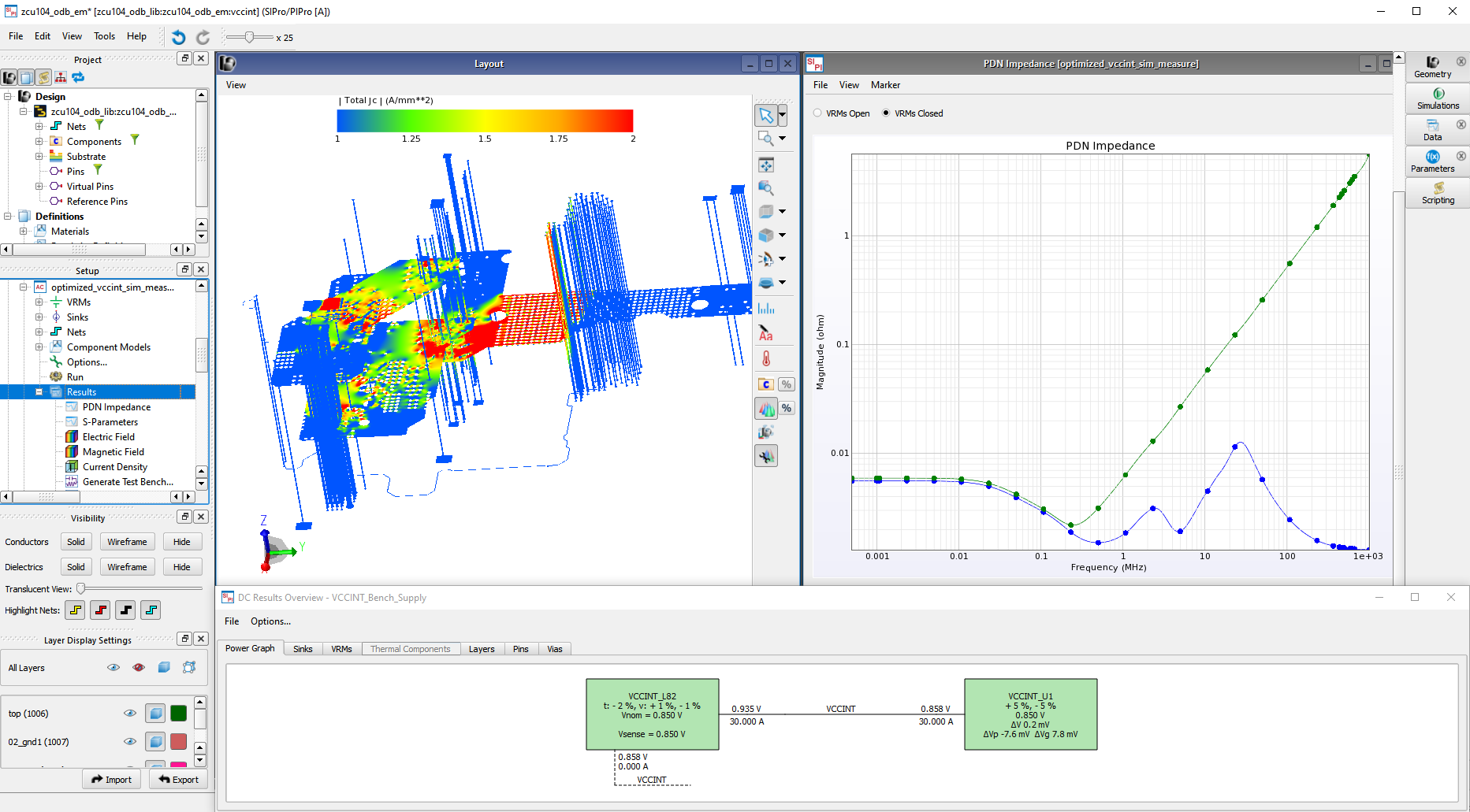
HB: Static is an average power or current draw and focuses on the DC IR drop. Dynamic is the transient response to a dynamic spectral content of the load and typically requires an EM model of the PCB to capture the distributed parasitics. I always recommend starting with the static DC IR drop to make sure the desired nominal voltage is reaching the load for a given average max current. Often sense lines are required to compensate for the resistive drop between the load and the VRM supply. DC IR drop simulators can help with the best location for a sense line when multiple loads are powered by the same PDN.
EM simulation tools like the Keysight’s PIPro in PathWave ADS make it easy to copy the DC analysis setup to an AC simulation for generation of the PCB PDN EM model. This model is typically a multiport S-parameter with the flexibility to quickly optimize the decoupling capacitor component values without rerunning the EM simulation. The EM model also is the key to doing full PI Ecosystem transient simulations in the time domain with dynamic loads and VRM behavioral models to identify worst case noise ripple for a given design.
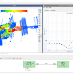
JS: What are the different challenges in analyzing the characteristic impedance (Z0) of power integrity (the frequency domain) and signal integrity (the time domain)?
HB: Jeff, I’m not sure if I would call power integrity frequency domain and signal integrity time domain. Both SI and PI operate in the time domain, but benefit from being designed and troubleshooted in the frequency domain. SI is about the time domain delivery of ones and zeros; power integrity is about delivering low ripple noise, free power in the time domain, to the load generating the ones and zeros. The SI world focuses on the impedance vs. distance (TDR) along the transmission line from the Tx to the Rx to avoid reflections and maximize the signal to the receiver. PI looks at impedance vs. frequency to ensure low noise ripple at all frequencies of excitation and to avoid resonances. In both cases, SI and PI benefit from matched impedance to get the best performance.
JS: Heidi, thank you for taking time today to share your insights into power distribution network (PDN) integrity in embedded systems.
HB: Jeff, thank you for the opportunity.
JS: Be sure to check out part one of this virtual interview, where I talk with Heidi about printed circuit boards, ground planes and thermal design considerations for power distribution networks for embedded systems.
About Heidi Barnes
Heidi Barnes is a Senior Application Engineer and Power Integrity Product Owner for High Speed Digital applications in the Design Engineering Software Group of Keysight Technologies. Her recent activities include the application of electromagnetic, transient, and channel simulators to solve signal and power integrity challenges. Author of over 20 papers on SI and PI, active member in developing the new IEEE P370 Standard involving interconnect S-parameter quality after fixture removal, and recipient of the DesignCon 2017 Engineer of the Year.
Prior experience includes seven years in signal integrity for ATE test fixtures for Verigy, an Advantest Group, eight years in RF/Microwave microcircuit packaging for Agilent Technologies, 10 years with NASA in the aerospace industry, and one year with Arco Solar in the solar cell industry. She has been with Keysight EDA software since 2012. She holds five patents, and was awarded the NASA Silver Snoopy for her work on hydrogen fire and gas detection.
Heidi graduated from the California Institute of Technology in 1986 with a bachelor’s degree in electrical engineering.

Leave a Reply