
Welcome to this Virtual Interview on power distribution network (PDN) integrity in embedded systems. We are here today with Heidi Barnes (HB), Senior Application Engineer for PathWave EDA for High-Speed Digital with Keysight Technologies. The following is from an interview with Heidi by EEWorld’s Jeff Shepard, where they discuss printed circuit boards, ground planes, and thermal design considerations:
JS: What are the main PDN considerations for printed circuit board layups in high-performance embedded systems?
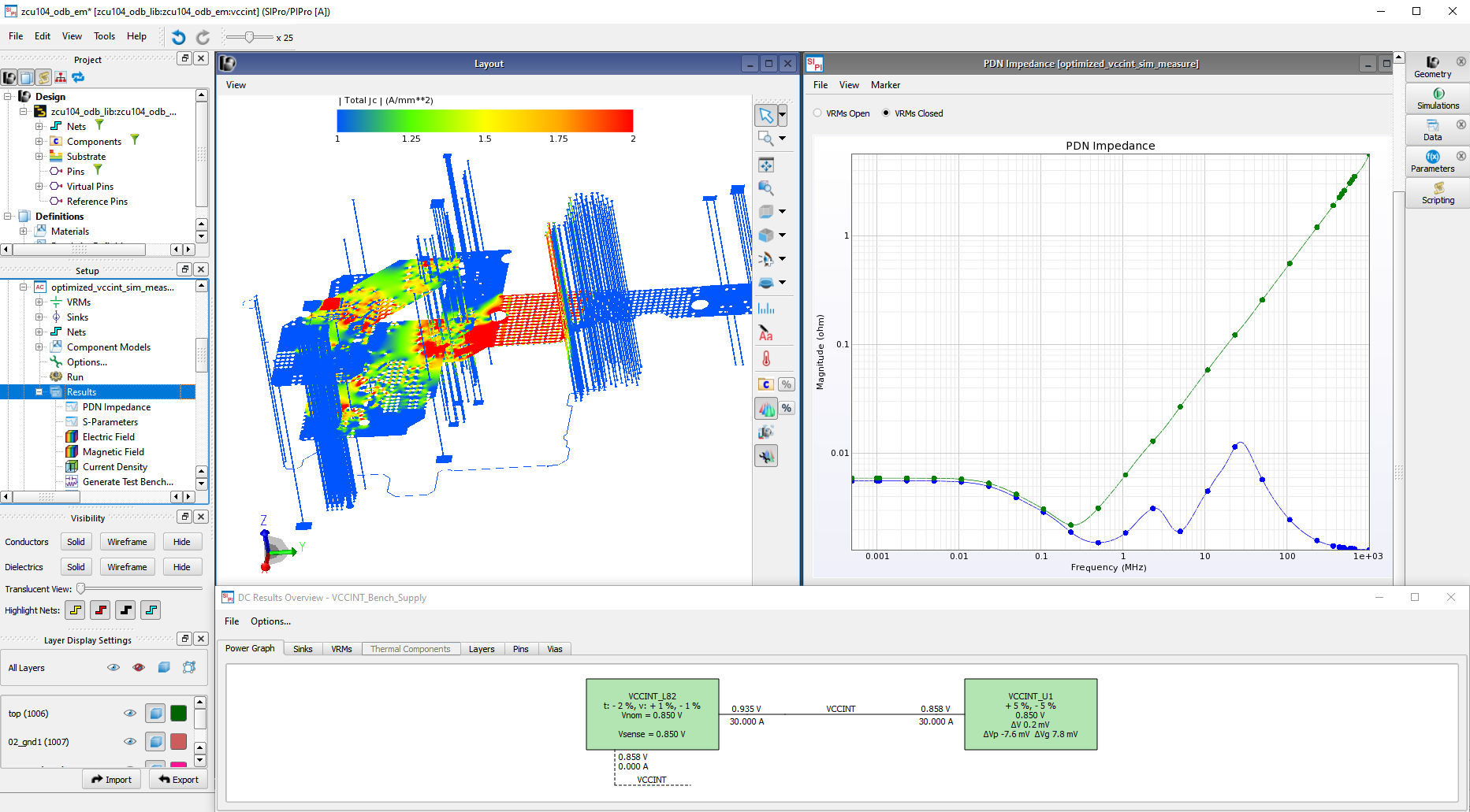
HB: Jeff, it will depend on the application, but one of the basic challenges is that delivering power to embedded systems with switching transistors at GHz speeds is not a DC problem. This is an AC challenge that has evolved into the world of power integrity, where one learns that PCB PDN impedance vs. frequency can be far more important than the simple DC resistance from the power supply to the load. The impedance of modern-day power-saving designs with lower and lower voltages can easily be degraded by PCB parasitics.

Inductance is the biggest challenge since any parasitic series inductance L times the dynamic current di/dt will result in noise ripple on the power rail. The PCB designer must fight to keep the power and ground close together to minimize this routing loop inductance. This means that PCB PDN’s for embedded systems would benefit from routing the PDN more like an AC transmission line rather than a simple DC net connection. EM simulators such as Keysight’s ADS with PIPro make it easy to analyze the PDN and help minimize the parasitic PCB loop inductances.
JS: Heidi, what is the most common error designers make when beginning PDN layouts?
HB: Forgetting where the return path is! Remember that “ground is for potatoes and carrots”, as I have often heard by EMI/EMC expert Bruce Archambeault. This is often a result of schematics that utilize the universal ground symbol to magically tie all the grounds together with no thought of the impedance of the actual routing and the potential for ground loops. Power should always be routed with an adjacent ground return; even via transitions between layers, benefit from having power and ground vias adjacent to each other to reduce the inductance. EM simulators can provide current density plots vs. frequency to quickly see how the parasitic PCB inductances change the flow of power as frequency increases.
JS: Heidi, how critical is the placement and geometry of ground planes?
HB: If your design can afford it, having power and ground plane layers with thin dielectrics on the order of a few mils between them can go a long way towards minimizing the loop inductance. Having the power and ground plane layers close together also reduces the path inductance when connecting to capacitors, which helps to make the capacitors less sensitive to placement. Having the power and ground layers as close to the device as possible can also reduce the loop inductance of the connecting vias. However, the layers at the top and bottom of the PCB are prime real-estate for high-speed routing. Overall system performance is better with the power and ground layers in the middle of the PCB, which also makes it easier for copper balancing.
Don’t forget – the more package capacitance a device has, the more inductance one can have on the PCB PDN. This means that sometimes the best solution is to pay a little extra for a device with more internal package PDN capacitance and reduce the routing constraints and number of capacitors on the PCB.
JS: How do thermal management considerations fit into PDN designs?
HB: Jeff, thermal run away is bad, and most designers can easily run checks to avoid excessive current densities. However, the bigger challenge is that poor thermal design can lead to lower reliability and increased field failures. The combination of electrical resistivity and thermal conductivity is not always intuitive. This is a great application for simulation. To do the iterative, solve between the changing resistance with temperature and then the subsequent change in current flow that changes the temperature. DC Electrothermal simulation tools can quickly identify routing issues and look at the trade-offs of increased copper thickness, the addition of multiple routing layers for a power rail and ground return, or the addition of heat sinks to target specific components.
JS: Heidi, thank you for taking time today to share your insights into power distribution network (PDN) integrity in embedded systems.
HB: Jeff, thank you for the opportunity.
JS: Be sure to check out part two of this virtual interview, where I talk with Heidi about the use of decoupling capacitors and other considerations when minimizing potential noise problems as well as static and dynamic analysis of PDNs in embedded systems.
About Heidi Barnes
Heidi Barnes is a Senior Application Engineer and Power Integrity Product Owner for High-Speed Digital applications in the Design Engineering Software Group of Keysight Technologies. Her recent activities include the application of electromagnetic, transient, and channel simulators to solve signal and power integrity challenges. Author of over 20 papers on SI and PI, active member in developing the new IEEE P370 Standard involving interconnect S-parameter quality after fixture removal, and recipient of the DesignCon 2017 Engineer of the Year.
Prior experience includes seven years in signal integrity for ATE test fixtures for Verigy, an Advantest Group, eight years in RF/Microwave microcircuit packaging for Agilent Technologies,10 years with NASA in the aerospace industry, and one year with Arco Solar in the solar cell industry. She has been with Keysight EDA software since 2012. She holds five patents and was awarded the NASA Silver Snoopy for her work on hydrogen fire and gas detection.
Heidi graduated from the California Institute of Technology in 1986 with a bachelor’s degree in electrical engineering.


Leave a Reply