Just one day after Yole Dévelopment released a report detailing a Power Integrations’ GaN-on-Sapphire HEMT IC found in the Anker‘s PowerPort Atom PD 1 wall charger (released at CES in January), the supplier of high-voltage integrated circuits for energy-efficient power conversion announced today the new family of offline CV/CC flyback, GaN-based InnoSwitch3 AC-DC converter ICs.
The InnoSwitch-CP (Constant Power), InnoSwitch3-EP (for open frame), and InnoSwitch3-Pro (digital control) ICs, boast lower switching losses, as well as lower RDS(on) per unit area than a conventional MOSFET— normally increased in GaN-HEMTs due to trapping effects. Additionally, the ICs GaN-based design achieves 95% full-load efficiency, allowing for the elimination of heatsinks from adapter designs and making it ideal for aftermarket USB PD adapters, high-end cellphone chargers and other mobile devices, notebook adapters, and other products with size or efficiency needs.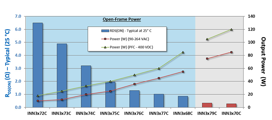
The quasi-resonant devices combine primary, secondary, and feedback circuits in a single surface-mounted package. In the newly released family members, GaN switches replace the traditional silicon high-voltage transistors on the primary side of the IC, reducing conduction losses when current is flowing, and considerably reducing switching losses during operation. This results in substantially less wasted energy and therefore increased efficiency and power delivery from the space-saving InSOP-24D package.
The new ICs provide accurate CV/CC/CP independent of external components and easily interface to fast-charging protocol ICs. The InnoSwitch3-CP and ‑EP variants are hardware-configurable, while the InnoSwitch3-Pro incorporates a sophisticated digital interface for software control of CV and CC setpoints, exception handing and safety-mode options.
The company maintains that because their strategy is to enclose and protect the GaN device within their ICs, engineers will see significant performance benefits but with the same simple flyback circuit topology and identical SMPS design flow as their silicon InnoSwitch3 ICs, identical switching frequencies, similar switching waveforms, and external components scaled for power. Circuit operation, according to the company, is indistinguishable from one using a silicon device.
“GaN is a pivotal technology offering significant efficiency and size benefits over silicon,” says Balu Balakrishnan, president and CEO of Power Integrations. “We anticipate a rapid conversion from silicon transistors to GaN in many power applications. InnoSwitch3 has been the clear technology leader in the offline switcher IC market since we launched the silicon variants 18 months ago, and the new GaN-based ICs further extend our lead by advancing both the efficiency and power capability of our flyback products.”
Power Integrations’ new InnoSwitch 3 ICs are available now, priced at $4/unit in 10,000-piece quantities. Five new reference designs describing USB-PD chargers from 60 W to 100 W are available on the Power Integrations website, along with an automated design tool, PI Expert, and other technical support documentation.
The IC mentioned in the Yole report is already designed in and commercially available in high-volume devices such as the Aukey and RAVpower chargers, in addition to the Anker PowerPort Atom PD 1. Watch a Charger Lab teardown of the Anker wall charger here.



[…] cheaper. This year, Power Integrations announced one of its sapphire-substrate GaN parts is used in an inexpensive “wall wart” charger. As a system engineer, you must understand that the greater cost of a GaN transistor will be offset […]