By Lluis Beltran Gil, Analog Devices
Several system-level techniques are available that can make signal chains designs more power efficient and reduce system design complexity.
Low-power signal chains are critical when designing a battery-powered measurement system for applications such as field instruments (sensing temperature, pressure, or flow) or remote vital sign monitoring devices. Even for mains-powered systems, minimizing the environmental impact of the energy costs pushes hardware designers to improve system power efficiency. A low-power design may have indirect benefits, like smaller solution size, if enabling to reduce the number of battery cells in parallel. A further advantage of the low-power design is the lower IC die temperature due to the lower energy the system consumes, thereby extending product lifetimes.
Precision low-power signal chains are a great starting point for quickly getting a low-power hardware design done. Beyond choosing low-power components, several power optimization techniques, such as power scaling, power cycling, and duty cycling, can be implemented to reduce the system’s power consumption further. Also, design choices like appropriate resistor values or memories can be a excellent differentiator for achieving stringent low-power targets and optimal battery life.
For example, identifying building blocks in the signal chain that can be eliminated or powered down momentarily when certain conditions are met makes it possible to implement low-power techniques. This will require a good timing analysis1, 2, and staging or duty cycling the operation. If several building blocks are idling for the greatest portion of the time, then these can be placed into shutdown mode or directly switched off. Note that fully power cycling a device will have some implications in terms of power and timing compared to shutdown modes when available.
Once this timing is implemented correctly, significant system-level power consumption improvements can be achieved even further by minimizing the microcontroller interaction. This will require using external or internal memories to store data while the host controller is shut down.
There are some differences in how to apply power-saving techniques at the system level, depending on the type of ADC used for digitizing the sensor information, among SAR and sigma-delta, as detailed in the following sections. Also, hardware design decisions like digital comms pull-up/pull-down resistors, resistive dividers, and gain setting resistors will make a difference in the overall signal chain power consumption.

Pin naming may vary from device to device. For consistency, we will refer to AVDD for analog supply, VIO for digital supply, and VREF for reference voltage.
Power optimization on a SAR ADC-based signal chain
SAR ADCs perform conversions on demand — that is, they toggle from sample mode to hold mode3 after the assertion of the CONVERSION START command. The conversion process starts, and once completed, it toggles back to sample mode to acquire the signal. SAR ADCs, like the AD4001 converter used in the signal chain shown in Figure 1, consume most of the power during the conversion phase, whereas consumption is minimal during the acquisition phase, as shown in Figure 2. So, despite being capable of throughputs as high as a few MSPS, power can be significantly optimized by running these converters at the minimum speed required by the application.
SAR ADC: power scaling with throughput
In many low-power applications, sensor information is not needed continuously but at much lower rates — on the order of kSPS or tens of kSPS. In these cases, power consumption of the SAR ADC can be scaled down with throughput, both for analog and digital supply rails.
| Application | Common Sampling Frequency |
| Field Instruments | 60 SPS to 600 SPS |
| Condition-Based Monitoring | 1 kSPS to 10 kSPS |
| Vital Sign Monitoring | <1 kSPS |
Table 1. Common Sampling Frequencies at Different End Applications
Most precision SAR ADCs have an internal clock that manages the conversion process, so the conversion time (tCONV) is fixed. With tCONV being set, the lower the throughput and the longer the cycle time (tCYC), the longer the acquisition time (tACQ), the period where the ADC minimizes its power consumption. In other words, the lower the throughput rate, the lower the power consumption per sample acquired.


Conversions are triggered externally through a digital signal so that the conversion speed can be tightly controlled. A slower sampling rate results in a longer acquisition phase and, therefore, a lower average power consumption. This can be observed in Equation 1:
Where:
- tCONV is the conversion time
- tCYC is the inverse of the sampling rate
- VDD is the analog supply
- VIO is the digital supply
- nBITS is the resolution of the ADC
- tSCLK is the serial clock period time (1/fSCLK)
- VREF is the reference voltage, and IREF is the current at maximum throughput (max_tput)
The ADC average analog power consumption will be inversely proportional to the sampling rate — according to Equation 1 and as seen graphically in Figure 4 — if tCYC is extended while tCONV remains constant.
The power consumption of the ADC shown in Figure 1 is dominated by the analog supply during its conversion phase, as shown in Figure 2. For example, in a strain gauge sensing circuit, the data acquisition rate can be as low as 1 kSPS, which reduces power consumption by 20-fold compared to running the AD4001 at maximum sampling speed.
| AD4001 Throughput Rate | Total Power Consumption |
| 1 kSPS | 300 μW |
| 10 kSPS | 400 μW |
| 1 MSPS | 6 mW |
Table 2. AD4001 Power Scales with Throughput
A graphical representation of Equation 1 shows how the power increases exponentially with throughput, as shown in Figure 4.
Reducing the ADC sampling rate results in a longer acquisition time, which reduces the bandwidth requirements of the ADC driver amplifier, allowing a larger base of devices to choose from. Lower bandwidth amplifiers tend to have comparatively lower quiescent current. Lower ADC sampling rates lower not only ADC power consumption but also lower power requirements for companion amplifiers.
| Op Amp | Bandwidth | IQ | eN |
| ADA4897-1 | 90 MHz | 3 mA | 1 nV/√Hz |
| ADA4610-1 | 16 MHz | 1.6 mA | 7.3 nV/√Hz |
| MAX40023 | 80 kHz | 17 μA | 32 nV/√Hz |
Table 3. Operational Amplifier Bandwidth vs. Current Consumption and Noise Performance; Bandwidth and Power Are Inversely Proportional
However, selecting a lower bandwidth operational amplifier has its trade-offs. The lower bandwidth means a lower quiescent current (IQ), but it comes at the expense of increasing the voltage noise density (eN), as shown in Table 3. As a rule of thumb, lowering the quiescent current implies that the noise density increases at a ratio of 1/√IQ. However, note that the rms noise will be filtered by the adjusted bandwidth. In other words, a hardware designer might trade off power consumption (or battery life) vs. rms noise performance for the given sample rate, amplifier, and RC net bandwidth.

Furthermore, the feedback resistors used to set the operational amplifier gain will also impact power consumption: the larger these resistors are, the less power they will consume. This, again, comes with a noise trade-off as larger resistors generate more noise. A good design practice is to make the resistors as large as possible but not large enough that their contribution to the total noise is substantial. As individual noise contributions are root sum squared for obtaining total noise, following a common rule of thumb would lead us to set a maximum limit for resistor noise rms of 1/3 of that of the op amp to keep their noise contribution less than 5% of the total. This would keep the op amp noise dominant.
In some applications where low-frequency input signals are sampled at low throughput rates (a few kSPS), like the ones shown in Table 1, the driver amplifier could be removed, if no signal conditioning, like a gain stage or low output impedance, is needed. In higher-speed applications, newer ADCs like the AD4000 or AD4696 families offer high input impedance (high-Z) modes that allow lower bandwidth (and lower power) amplifiers to drive the analog inputs, sometimes even eliminating the driver. Removing this op amp will also minimize total power consumption by eliminating its contribution, as indicated by the blue bar portion shown in Figure 5. This results in significant power savings compared to traditional SAR ADCs that almost always require a driver amplifier. In the case of the AD4696, a 16-channel device, this power savings is multiplied by 16 times. The reference high-Z mode feature reduces the reference input current and the overall system power consumption.
SAR ADC signal chain: AFE dynamic power scaling
As described in the previous section, SAR ADC power consumption inherently scales with sample rate, but this is not true for other signal chain components. Amplifiers and voltage references consume constant quiescent current while they are powered up. Power cycling these components between ADC samples reduces the average power consumption of the signal chain. Waiting for signals to be settled on every power cycle limits the time left for powering the system on and off. This is well explained in “What Are the Most Important Timing Factors for Low Power Precision Signal Chain Applications? Part 1”and “What Are the Most Important Timing Factors for Low Power Precision Signal Chain Applications? Part 2”(although an accurate analysis for each particular signal chain design is recommended).
Using highly integrated ADCs, with more analog front-end (AFE) blocks on chip, enables faster power-up and power-down transitions without compromising the performance. However, in many scenarios, a design may use discrete components for optimal performance. An example is shown in Figure 6.
This signal chain is multichannel and is comprised of one MAX41400 plus one antialiasing filter per channel, feeding into a
16-channel SAR ADC (the AD4696) with an ADR3625 precision reference.
As shown in the previous section, running the ADC at the lowest acceptable throughput reduces its power consumption. Beyond that, if the idle time is large enough, the amplifier can be put into shutdown mode during a portion of the acquisition time, given that for a multiplexed system like this, only one amplifier needs to be powered up at a time. The frequency at which the amplifier needs to be powered up is tCYC/LSEQ, where LSEQ is the length of the sequence, which is ten in the example given in Figure 7. For example, if running conversions at 1 kSPS per channel and the conversion time is a maximum of 415 ns, the amplifier on each channel can be placed into shutdown mode for around 10% of the cycle time.


The quiescent current (IQ_ON) of the amplifier is 65 μA when fully powered up, but it can be reduced to 0.1 μA when placed into shutdown mode (IQ_OFF). The average current consumed (IAVG) by the amplifier can be scaled with throughput by powering it down in between samples.
Once again, the slower the throughput, the higher the tCYC, and the lower the IAVG. tON is the time during which the amplifier is turned on. When the ADC switches from the acquisition to conversion phase, the amplifier can be powered off, as extending tON longer than the minimum required does not yield any benefit. This off-time (tOFF = tCYC – tON) should be maximized for minimum power consumption, not to the extent of compromising SNR or THD. Finding the right timing will depend on the application, the devices used, and the throughput rates. In fact, tON and throughput are inversely proportional: lower throughputs lead to longer idle time, and longer idle time requires longer tON to power the amplifier back up. Based on the datasheet, the typical conversion time of the SAR ADC is 415 ns. This conversion time plus the 100 μs required to power up the amplifier after shutdown will add up to the minimum tON time. So, the average current consumption will be:
Compared to an amplifier that is always enabled, the shutdown modes and fast power-up time of the MAX41400 result in a
10× reduction in current consumption.
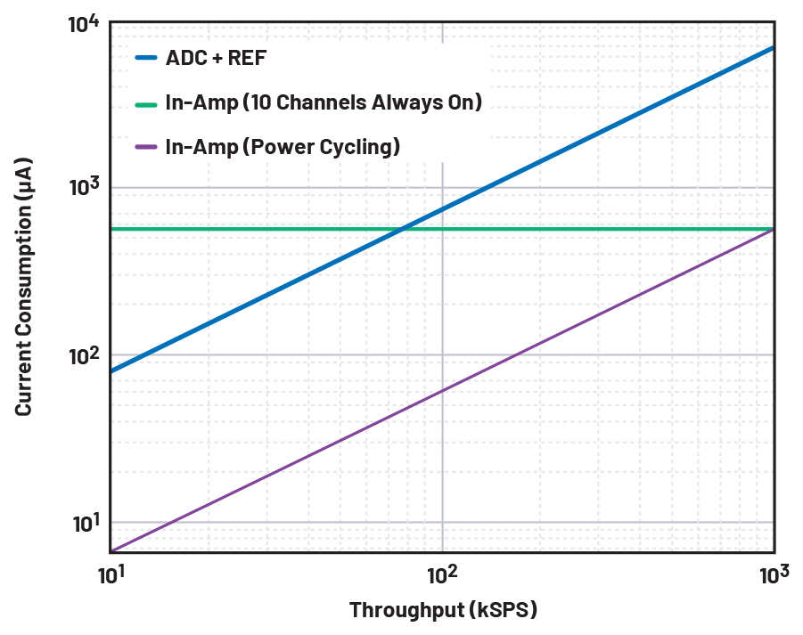
For a more general view, besides power savings calculated on the examples shown so far at a given throughput rate, all these equations can be represented graphically as in Figure 9, with the specifications taken from the data sheets (assuming reference and analog input high-Z mode are enabled).

This same analysis can be done for battery life instead of power consumption by dividing the battery capacity by the average current drawn.
| Battery | Capacity (mAh) |
| CR927 | 30 |
| 2× LR44 | 158 |
| 2× AAA | 1000 |
| CR2354 | 560 |
Table 4. Batteries’ Capacity
In this case, the relationship is inversely proportional—the lower the throughput, the longer the battery will last.

Any amplifier, even if it does not have a shutdown mode, can be power cycled. That is, powering it on and off entirely instead of entering shutdown mode. However, care must be taken. On the one hand, the wake-up time will be longer to get the amplifier ready so that the minimum tON will be longer. On the other hand, charging and discharging the decoupling capacitors repeatedly will have implications on the current drawn to charge them up every power cycle, increasing the overall power consumption compared to using shutdown modes. Also, if the sensor is still driving the amplifier inputs while the rails are not powered up, this may lead to damage if they are unprotected.
SAR ADC-based signal chain: digital supply power scaling
The previous section focused on reducing the analog supply power consumption, given it is the maximum contributor to the total power consumption. Reducing the throughput also has an impact on the digital power consumption as it allows the serial clock to run at a lower frequency:
Equation 5 indicates that there are two extra potential steps we can take to minimize digital power consumption:
- Use a lower digital supply voltage (VIO)
- Minimize the trace capacitance of the serial data output line
Another point to note is the value of the pull-up/pull-down resistors used in the digital communication lines. These resistors ensure a proper logical level at the digital input/output, and their value may impact the overall system power consumption. Using too low a resistor value, also known as strong pull-up, will cause a high current to flow through it. Hence, unnecessarily low values should be avoided. On the other end, if the resistance is too high, the voltage drop caused by the leakage current could result in the interpretation of an incorrect logic level. In addition, the voltage drop impacts the propagation. Designers must use the highest resistor value without compromising the voltage level (this will depend on the digital supply voltage and leakage current) or the signal integrity.
Sigma-Delta ADC-based signal chain
In the case of sigma-delta ADC-based signal chains, the power scaling concept described in previous sections is not applicable straight away. This is because conversions are not externally triggered; instead, they work from a free-running clock.4 They cannot remain idle for a certain period of time as a function of an external conversion start signal.
However, many sigma-delta ADCs feature standby modes that can be used if the ADC does not need to convert continuously. As in previous sections, timing considerations5 need to be considered as recovering the device from standby mode requires a wake-up time during which no samples can be taken.
Highly integrated sigma-delta ADCs offer duty cycling and standby modes. That way, the ADC powers up and down automatically without the need to interact with the host every cycle. The AD4130 offers two modes, 1/4 and 1/16, which means it is active during 1/4 or 1/16 of the time. That leads to significant power reduction compared to continuous conversion mode, as shown in Figure 10.
| AD4130 Power Mode | Typical Current Consumption |
| Continuous Conversion | 32 μA |
| Duty Cycling | 5 μA |
| Shutdown Mode | 0.5 μA |
Table 5. AD4130 Current Consumption for Each Power Mode
Depending on the required throughput rate, techniques for optimizing power consumption can be either using one of the duty cycling modes or just putting the part into standby mode for a given period. Indeed, the AD4130 has many operating modes that may impact power consumption of the ADC. The active functional model in ACE6 shows the power consumption and the expected battery life for the selected ADC configuration.

Sigma-Delta ADC-based signal chain: AFE dynamic power scaling with duty cycle
Just as with the SAR ADC-based signal chain, a sigma-delta-based signal chain can take advantage of the duty cycle to power down certain blocks when the ADC is placed into a low-power state (Figure 10). That would allow AFE power savings similar to the ones shown in Figure 9.
Sensor excitation
A complete solution provides the core converter, the internal programmable gain amplifier, and sensor biasing and excitation (selectable current source and precision voltage reference). This integration has implications in terms of ease of use, size, and optimization on biasing, timing, or power cycling among the different building blocks. The ADC reduces the overall system power consumption by housing all these blocks on chip. Furthermore, it simplifies the design cycle thanks to its flexibility in many different platforms like RTD, thermistor, or bridge sensors, to name a few. It also reduces the BOM count and the need for several power supply rails.
Other power optimization techniques
Throughout this article, several ways to minimize the signal chain power consumption have been presented. However, one portion of the signal chain has not been considered yet is the host controller. If the controller is powered up all the time because it needs to read and post-process data from the ADC, it will sink a good portion of the power. Placing the controller into sleep mode while not in use will help achieve extra power savings.
ADCs with on-chip FIFO
If the application does not need real-time data but must read data points at a much lower rate, ADCs with on-chip FIFO might play a role. The AD4130 incorporates such a block, and this FIFO can store up to 256 conversions, so if the output data rate (ODR) is, for example, 2.4 kSPS, instead of reading every 416 μs, the microcontroller can be put to sleep mode and wake up every 100 ms to read the whole data memory in one go (see the Data Transfer section in Figure 11). In other words, having an ADC with memory that stores up to the latest 256 samples also enables power cycling of the microcontroller, thereby drastically reducing the overall system power consumption.

Streaming ADC data to memory through Direct Memory Access (DMA)
An alternative for ADCs that do not include on-chip FIFO would be to use the direct memory access (DMA) available in most microcontrollers. DMA enables the passing of data directly from a peripheral (in this case, the SPI) to memory (SRAM) without CPU intervention or interrupts for every single ADC sample received. The chosen microcontroller will have a direct impact on achievable power savings. In many cases, the microcontroller can stay in sleep mode most of the time and trigger an event only when an ADC sample is received. This event will then briefly alert the DMA to start performing the SPI transactions and to return to sleep after that, thus minimizing the microcontroller power consumption compared to having the CPU fully awake for the whole SPI transaction. Note that using the DMA is only applicable if the format of the ADC data matches the destination memory. For most microcontrollers, the DMA can be easily used only when the ADC data is 16 or 32 bits long.
Interrupt-driven programming
Many low-power applications do not require the recording and processing of every single data point but rather monitoring that the magnitude sensed is within certain thresholds. Traditionally, to do this, the host controller needed to be constantly awake to read each ADC sample and decide if the value was acceptable or not. Consequently, it would trigger an interrupt routine if need be.
Thresholds can be programmed such that a GPIO pin asserts only if the ADC output code is out of the user-defined bounds. This way, the host controller can stay in sleep mode most of the time and only wake up when the GPIO asserts, minimizing its power consumption, given it will only be active when it is necessary to perform an action.
Conclusion
When designing a battery-powered measurement system for applications such as portable field instruments, condition monitoring, or vital sign measurements (VSM), low-power signal chains are ideal for achieving power-optimized solutions. Analog Devices’ precision low-power signal chains ease the journey for designers building low-power measurement solutions, which offer the optimal combination of precision amplifiers, voltage references, ADCs, and isolation products. In these signal chains, power consumption is optimized while keeping noise performance, size, and ease of use as key vectors. These signal chains come in different flavors: single-channel, discrete multichannel (multiplexed), fully integrated multichannel solutions, and ready-to-go power-optimized designs, offering an excellent starting point for low-power design.
References
[1] Padraic O’Reilly. “What Are the Most Important Timing Factors for Low Power Precision Signal Chain Applications? Part 1.”
Analog Dialogue, Vol. 56, No. 3, August 2022.
[2] Padraic O’Reilly. “What Are the Most Important Timing Factors for Low Power Precision Signal Chain Applications? Part 2.” Analog Dialogue, Vol. 56, No. 3, August 2022.
[3] The Data Conversion Handbook. Analog Devices, Inc., 2005.
[4] Michael Clifford. “Fundamental Principles Behind the Sigma-Delta ADC Topology: Part 1.” Analog Devices, Inc., January 2016.
[5] Bruce Pepitas. “Introduction to Dynamic Power Scaling.” Analog Devices, Inc., January 2016.
[6] Analysis | Control | Evaluation (ACE) Software. Analog Devices, Inc.
[7] Brandon Hurst. “How to Accelerate Peripheral Monitoring in Low Power Wearables with DMA.” Analog Dialogue, Vol. 56, No. 1, January 2022.
[8] Maithil Pachchigar and Alan Walsh. “Next-Generation SAR ADC Addresses Pain Points of Precision Data Acquisition Signal Chain Design.” Analog Dialogue, Vol. 50, No. 4, December 2016.
[9] Sanjay Rajasekhar and Arvind Shankar. “How to Leverage Input High-Z Technology to Reduce Solution Power and Size.” Analog Devices, July 2022.


Leave a Reply