New converter topologies and power transistors promise to reduce the size and boost the efficiency of supplies that will run next-generation AI platforms.
Alex Lidow | Efficient Power Conversion
Artificial Intelligence (AI), gaming, cloud computing, and autonomous vehicles all employ the latest generation of graphics processors (GPUs) in lieu of CPUs. The reasoning is that GPUs offer higher computational density than traditional CPUs in terms of acquisition cost, size, and power requirements.
The implications for power architecture seem clear; trends in vehicular power design are increasingly influenced by the power demands of electronics for autonomous systems. AI-based vehicles on the drawing boards generally use 48 V as the dominant voltage on the board with the GPU, and the final voltage must be somewhere around 1 V or less. Power levels are already around 1.5 kW and could soon hit 3 kW per GPU. What is less clear is the architecture necessary for getting from 48 V to 1 V at these power levels.
There is a case for having isolation between the 48-V input and the point-of-load (POL) converters. It stems from two requirements. The first comes from the telecom industry where 48-V backup batteries supply a minus 48-V rail that must be isolated from the positive rails necessary to run the digital electronics. The second requirement stems from the range of voltages that might be seen at the nominally 48-V rail. With a range of 36 to 72 V, safety considerations dictate a need for isolation. Limiting the input range to less than 60 V eliminates the isolation requirements.
 Reducing the input voltage range to between 36 and 60 V (or even less in many cases) also reduces regulation requirements. The primary question is whether it is more economical or efficient to regulate at both the 48 VIN – X VOUT supply and the POL converter, or whether the burden of precise regulation can go only on the POL with the first stage delivering an output voltage proportional to the input voltage. There is no universal right answer to this question, but there are more and more applications that do not require the first stage regulation and operate as dc transformers (DCX).
Examining candidate architectures
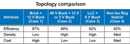
We will examine four different architectures as well as a spectrum of intermediate bus voltages: The more traditional 48-to-12-V isolated and regulated “brick” followed by a non-isolated 12-to-1-V buck converter; A regulated, non-isolated 48-to-12-V and 48-to-5-V buck converter, followed by a 12 or 5-to-1-V buck converter; An un-regulated 48-to-12-V or 48-to-6-V LLC (inductor-inductor-capacitor) topology, followed by a 12 or 6-V buck converter and, a regulated single-stage hybrid converter that goes from 48-to-1 V without an intermediate stage.
We start by examining the initial stage of conversion, then look at second-stage efficiencies at various voltages. These results can lead to conclusions about which architecture is most efficient, has the highest power density, and costs the least.
Isolated brick-format dc-dc converters are widely used in applications that need high reliability, efficiency, and robust performance in complex systems. The isolation takes place via a transformer. This approach has the twin benefits of providing a voltage transformation along with complete separation of input and load ground planes. The former helps maximize efficiency, and the latter is useful for both safety and to prevent or mitigate EMI and ground-loop problems.
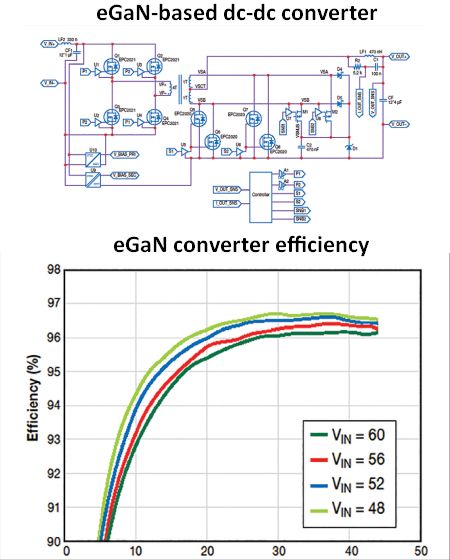
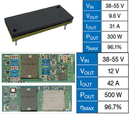
The state-of-the-art in a DOSA (Distributed-power Open Standards Alliance) standard eighth-brick converter is arguably a design using eGaN FETs. The basic design is a hard-switched, fully regulated PWM 48:12-V buck converter with a full-bridge input and a center-tapped synchronous rectifier output. Typical silicon-based eighth-brick converters show maximum output power levels near 300 W and peak efficiencies of approximately 96%. Such converters include custom heat sinks to function at these high-power levels. Such converters typically run at 150 kHz to 175 kHz to mitigate switching losses.
The low switching loss of the GaN transistors permit a doubling of the switching frequency to 300 kHz, which allows a great reduction in inductor and transformer size and a large boost in output current and power. The resulting converter is capable of fully regulated operation at an output current of 42 A, or 500 W at a 12-V output. It has realized a peak efficiency of 96.7% at 30 A (the max load current of the silicon-based converter), with a full-load efficiency of 96.4%.
The transistors account for 28% of the total loss (approximately 1% of the total output power). On the other hand, the magnetic components account for > 48% of the total loss. Thus the transistors are no longer the main limiting factor in the converter design.
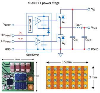
Non-isolated dc-dc converters can be physically small, efficient, and cost effective when based around GaN FETs. In one case, a 25-A, 48 V to 5-12-V converter was constructed using the EPC2053 eGaN FET. The EPC9093 GaN development board, configured as a synchronous buck converter, yields a main power stage area of only 10×9 mm, which is half the size of its silicon equivalents, and can produce an output voltage ranging from 5 to 12 V.
The EPC2053 is a Generation 5 eGaN FET rated at 100 V with a 3-mΩ typical on-resistance capable of carrying a 32-A continuous current and operating with up to a 150°C junction temperature. The EPC2053 has lower parasitic capacitances and on-resistance than its silicon counterparts, yielding faster switching and lower power losses even at higher switching frequencies. These qualities enable compact converters to produce high output power.
When stepping down 48 V to 12 V at a 700 kHz switching frequency, the EPC9093 hits a peak efficiency of 97% when powering a 15-A load and maintains the efficiency above 96.5% with a 25-A load.
The 48-V step-down LLC dc transformer employs the LLC topology to provide a high-power density and high efficiency in dc-dc power conversion. This converter can maintain a high efficiency over a wide operating range when operated as a dc transformer with a fixed conversion ratio, making it well suited for applications having relaxed requirements for output voltage regulation. The LLC can operate at frequencies high enough that parasitic elements can serve as circuit components, helping to minimize the physical component count.
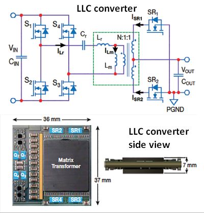
A nearby figure shows the schematic of a N:1 full-bridge LLC converter with a center-tapped synchronous rectifier. This circuit operates with ZVS for all the switching devices. The primary side devices are EPC2053 transistors, and the secondary rectifiers are the 1.15-mΩ-typical, 30-V-rated EPC2023.
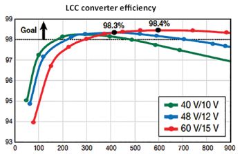
A 1-MHz, 900-W-capable, 48-to-6-V LLC converter has also been designed with an 8:1 ratio transformer using a 14-layer PCB and with a magnetizing inductance of 2.2 µH. The primary side devices are EPC2053 transistors and the secondary rectifiers are the 1.15-mΩ-typical, 30-V-rated EPC2023, with each rectifier having two devices connected in parallel.
A new 48-to-1-V Dual Inductor Hybrid Converter (DIHC), based on the Dickson switched-capacitor converter, has been proposed to address the drawbacks of conventional approaches. The DIHC employs two interleaved inductors at the output and eliminates two large synchronous switches in the hybrid Dickson converter. These modifications let switch conduction and flying capacitors contribute nearly 2X less to the dc output impedance compared to the hybrid Dickson converter and thus 2X smaller conduction losses than the hybrid Dickson converter.
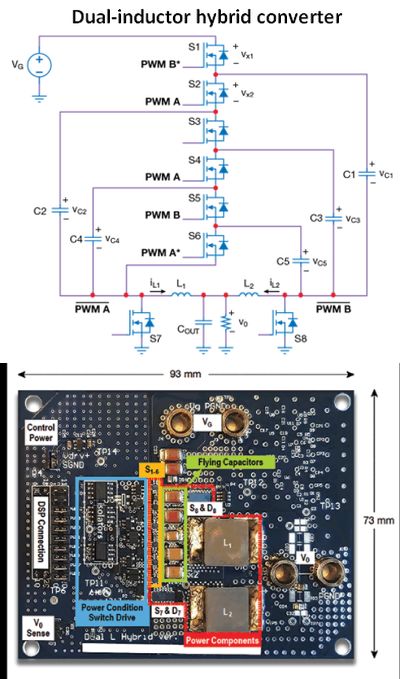
In addition, the two interleaved inductors with naturally self-balanced currents give the DIHC the same benefits as in multi-phase converters for high-current applications without additional current balancing complexity. The DIHC also uses a split-phase operation to realize complete soft-charging for all the capacitors.
A key benefit of the DIHC is that all flying capacitors are soft-charged/discharged by inductor currents without a hard-charging mode. Because flying capacitors see complete soft-charging, the DIHC can use significantly smaller capacitors without a higher switching frequency. In addition, the inductors can be favorably sized for high power density because of the reduced switch voltage. The smaller capacitors and inductors give the DIHC a high power density and looks promising for high-power and high current applications.
Optimizing the intermediate bus voltage
We can now turn to the efficiency of the second stage. Multiplying the peak reported efficiency of various commercial POL converters with the efficiency of the first stage converters gives a reasonable estimate of comparative peak efficiencies going from 48 to 1 V.
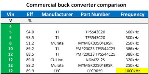 The best efficiency comes from coupling either the DIHC or the LLC with a 6-VOUT second stage. The DIHC topology, however, is relatively new and has yet to be widely adopted. New AI and gaming applications are quickly adopting the 48-VIN-to-6-VOUT LLC, coupled with a 6-VIN-to-1-VOUT buck converter because of its high efficiency, high power density, and low cost. Traditional bricks are going to be around for many more years but are probably not going to see much growth in leading-edge high-density computing systems.
In all the topologies with 48 VIN, the highest efficiency comes with using GaN devices. This is due to their lower capacitance and smaller size. With recent pricing declines in GaN power transistors, the cost comparison with silicon-based converters now strongly favors GaN in all the leading-edge solutions.
REFERENCES
State-of-the-art in DOSA-standard eighth-brick converters: Glaser, J., Strydom, J. and Reusch, D., “High Power Fully Regulated Eighth-brick DC-DC Converter with GaN FETs,” in PCIM Europe 2015; International Exhibition and Conference for Power Electronics, Intelligent Motion, Renewable Energy and Energy Management; Proceedings of, 2015, pp. 406–413.
Non-isolated dc-dc converters: A. Lidow, J. Strydom, M. de Rooij, D. Reusch, “GaN Transistors for Efficient Power Conversion,” Second Edition, Wiley, 2014.
“Boosting Power Density in 48 V to 5-12 V DC to DC Converter Using EPC2053, with up to 25 A Output,” How2AppNote 009
48-V step-down LLC dc transformer: “Exceeding 98% Efficiency in a Compact 48 V to 12 V, 900 W LLC Resonant Converter Using eGaN FETs,” How2AppNote 011.
“How to Exceed 98% Efficiency in a Compact 48 V to 6 V, 900 W LLC Resonant Converter Using eGaN FETs,” How2AppNote 014,
N:1 full bridge LLC converter: Huang, H., “Designing an LLC Resonant Half-Bridge Power Converter,” Reproduced from 2010 Texas Instruments Power Supply Design Seminar SEM1900, Topic 3, TI Literature No. SLUP263
Ahmed, M. H., Fei, C., Lee, F. C. and Li, Q., “48V voltage regulator module with PCB winding matrix transformer for future data centers,” IEEE Trans. Ind. Electron., vol. 64, no. 12, pp. 9302-9310, Dec. 2017.
48V-to-1V Hybrid Converter: G.-S. Seo, R. Das, ad H.-P. Le, “A 95%-efficient 48 V-to-1 V/10 A VRM hybrid converter using interleaved dual inductors,” in Proc. IEEE Applied Power Electronics Conference and Exposition (ECCE), 2018. pp. 3825-3830
Y. Lei, R. May, and R. Pilawa-Podgurski, “Split-Phase Control: Achieving Complete Soft-Charging Operation of a Dickson Switched- Capacitor Converter,” IEEE Transactions on Power Electron., vol. 31, no. 1, pp. 770-782, 2016.
D. Baba, “Benefits of a multiphase buck converter,” Texas Instruments Inc., 2012.




Leave a Reply