• Skip to primary navigation
  • Skip to main content
  • Skip to primary sidebar
  • Skip to footer
  • Subscribe
  • Advertise

Power Electronic Tips

Power Electronic News, Editorial, Video and Resources

  • Products
    • Power Supplies
    • AC-DC
    • DC-DC
    • Battery Management
    • Capacitors
    • Magnetics
    • MOSFETS
    • Power Management
    • RF Power
    • Resistors
    • Transformers
    • Transistors
  • Applications
    • 5G
    • AI
    • Automotive
    • EV Engineering
    • LED Lighting
    • Industrial
    • IoT
    • Wireless
  • Learn
    • eBooks / Tech Tips
    • EE Training Days
    • FAQ
    • Learning Center
    • Tech Toolboxes
    • Webinars & Digital Events
  • Resources
    • Design Guide Library
    • Digital Issues
    • Engineering Diversity & Inclusion
    • LEAP Awards
    • Podcasts
    • White Papers
    • Design Fast
  • Video
    • EE Videos & Interviews
    • Teardown Videos
  • EE Forums
    • EDABoard.com
    • Electro-Tech-Online.com
  • Engineeering Training Days
  • Newsetter Subscription

What is the MOSFET body diode?

December 15, 2016 By Joshua Israelsohn

Unlike virtually every other active device, the power MOSFET is unusual in that its schematic symbol includes a parasitic device – the body diode. The body diode is intrinsic to the device’s structure. It remains despite a number of fundamental changes in power MOSFET structure and device designs including the two most common types today — planar and trench devices.

MOSFET schematic
MOSFET schematics, complete with body diodes.

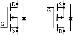
The presence of the body diode as an explicit element of the schematic symbol is an oddity. After all, we don’t pepper the MOSFET symbol with any of the three primary parasitic capacitances though they, too, affect the switch’s dynamic performance and, under suitable circuit conditions, lead to switching faults. But the body diode’s presence and behavior have become so much a part of the overall MOSFET device qualities that common circuit topologies depend on, or at least anticipate, the parametric performance of the parasitic component.

Discreet power MOSFETs also feature a parasitic bipolar transistor, but the metallization connecting the source and body regions — also an explicit feature of the schematic symbol — shorts the base-emitter junction. This prevents the bipolar device from turning on under all but the most extreme conditions. The remaining base-collector junction is in parallel with, and behaves essentially as part of, the body diode.

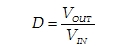
Many of the most common power MOSFET applications involve devices, in either half- or full-bridge configurations, driving inductive loads. Buck-converter topologies are a typical example. The high-side FET operates with a duty cycle D approximately equal to
duty cycle equation

buck converter
A typical buck converter topology.

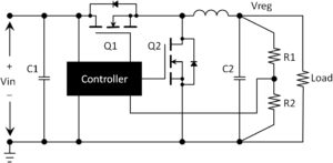
When the high-side switch turns off, the inductor current has ramped to its peak for the given clock cycle. The controller will impose an amount of dead time between the high-side MOSFET turning off and the low-side device turning on to prevent shoot through (rail-to-rail conduction through the half bridge). Nonetheless, the inductor will try to maintain its current, pulling the switching node negative until the low-side MOSFET’s body diode conducts. Even after the low-side switch turns on, the body diode doesn’t turn off for a period trr, the reverse recovery time, during which charges within the PN device must recombine.

Two parts of the MOSFET’s loss model are associated with the body diode in this scenario. The first is an IL∙VD term during the diode’s conduction interval. This is significantly larger than the switch’s I2∙RDS(on) loss — one motivation to minimize the switching dead time. The second is the recombination current, which adds to the inductor current flowing through the switch’s RDS(on). This results in slightly higher I2R losses than the circuit’s external behavior would suggest and a correspondingly higher operating temperature for the switch. Because RDS(on) exhibits a positive TCR (temperature coefficient of resistance), the device dissipation rises further, beyond that which constant-temperature calculations would predict.

Schottky diode in converter
A Schottky diode connected in parallel with a MOSFET body diode.

Should the switching dynamics and thermal performance fall short of your circuit’s requirements, or if you’re designing for maximum energy efficiency, you can essentially eliminate the body diode’s contribution to the switch’s behavior. A Schottky diode connected in parallel to the body diode will conduct with a lower forward voltage, preventing the body PN junction from becoming forward biased. The Schottky diode is a majority-carrier device and exhibits no recombination. Be sure to use short, wide traces to connect the Schottky and the MOSFET. Even small stray inductances can reduce the Schottky diode’s effectiveness.

You may also like:


  • Protecting fast EV charging stations

  • The evolution of smart MOSFET technologies

  • Advanced power electronics packaging

  • Increasing power conversion efficiency with new semiconductor technologies
  • thermal management
    Basic principles of thermal management

Filed Under: FAQ, Featured, MOSFETS Tagged With: body diode, MOSFET

Reader Interactions

Trackbacks

  1. 30 Best Power Electronics Project Ideas for Engineering Students says:
    September 10, 2022 at 8:00 pm

    […] A very effective and dependable non-isolated bidirectional DC-DC converter solution is put forth. A tiny negative coupled inductor is employed to divide the switch branch of the system into two power flows. Additionally, it stops electricity from passing freely through the MOSFET’s diode. […]

Primary Sidebar

Featured Contributions

Robust design for Variable Frequency Drives and starters

Meeting demand for hidden wearables via Schottky rectifiers

The case for vehicle 48 V power systems

GaN reliability milestones break through the silicon ceiling

Developing power architecture to support autonomous transportation

More Featured Contributions

EE LEARNING CENTER

EE Learning Center

EE TECH TOOLBOX

“ee
Tech Toolbox: Internet of Things
Explore practical strategies for minimizing attack surfaces, managing memory efficiently, and securing firmware. Download now to ensure your IoT implementations remain secure, efficient, and future-ready.

EE ENGINEERING TRAINING DAYS

engineering
“power
EXPAND YOUR KNOWLEDGE AND STAY CONNECTED
Get the latest info on technologies, tools and strategies for EE professionals.
“bills

RSS Current EDABoard.com discussions

  • About IF transformers.
  • LV25-P sensor help
  • ISL8117 buck converter blowing up
  • Mains inverter with switching node going out on the mains cable!?
  • avoiding mixer compression when acting as a phase detector

RSS Current Electro-Tech-Online.com Discussions

  • What part is this marked .AC ?
  • Photo interrupter Connections
  • How to balance Milwaukee M18 tool batteries
  • 20W Power Supply for Stereo Amplifier
  • FSK SER on the same symbols

DesignFast

Component Selection Made Simple.

Try it Today
design fast globle

Footer

EE World Online Network

  • 5G Technology World
  • EE World Online
  • Engineers Garage
  • Analog IC Tips
  • Battery Power Tips
  • Connector Tips
  • DesignFast
  • EDA Board Forums
  • Electro Tech Online Forums
  • EV Engineering
  • Microcontroller Tips
  • Sensor Tips
  • Test and Measurement Tips

Power Electronic Tips

  • Subscribe to our newsletter
  • Advertise with us
  • Contact us
  • About us

Copyright © 2025 · WTWH Media LLC and its licensors. All rights reserved.
The material on this site may not be reproduced, distributed, transmitted, cached or otherwise used, except with the prior written permission of WTWH Media.

Privacy Policy