
This year’s IEEE International Electron Devices Meeting (December 7-11, 2019) played host to presentations describing advances in gallium-nitride technology that may lead to smaller, more integrated power circuitry such as single-chip switching power supplies and more efficient power transistors.
The IEDM is considered one of the premier technical conferences for developments in semiconductor and integrated
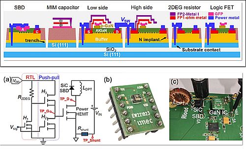
circuit technologies. One of the power-related papers delivered this year was from researchers at the Belgium-based nanotechnology center called Imec and Katholieke Universiteit Leuven (Paper 4.4, “GaN-on-SOI: Monolithically Integrated All-GaN ICs for Power Conversion,” X. Li et al.). They devised monolithically integrated GaN-on-SOI ICs for power conversion. The ICs comprised a complete buck converter that demonstrated 200 V on-chip power conversion at 1 MHz.
The researchers used an SOI (silicon-on-insulator) substrate because it eliminates a back-gating effect which wastes power. It also suppresses parasitics, provides electrical isolation, and reduces the chip area needed to host the power circuit. The team investigated the technology from the standpoints of substrate, buffer, isolation, device, co-integration and circuitry. The chip’s monolithically integrated components included a HEMT, a Schottky barrier diode, a MIM (metal-insulator-metal) capacitor, a 2DEG (two-dimensional electron gas) resistor, and resistor-transistor logic.
Another paper described advances made in GaN-on-Si technology that yielded a high breakdown voltage and low on-
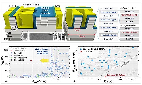
resistance (Paper 4.1, “1200 V Multi-Channel Power Devices with 2.8 Ω⋅mm ON-Resistance,” J. Ma et al.). Researchers from Ecole polytechnique fédérale de Lausanne (EPFL) in Switzerland and Enkris Semiconductor in China were able to devise lateral multi-channel AlGaN/GaN power devices with a 3.2 GW/cm2 figure of merit arising because of a high (1,230 V) breakdown voltage and low (2.8 Ω⋅mm) on-resistance. The researchers call these devices MOSHEMTs. They have a multi-channel FinFET-like architecture with slanted tri-gates whose structure can be modified to “tune” device performance.
The on-resistance is some 5x lower than previously seen at this breakdown voltage with single-channel devices. The researchers say until now, it has proven difficult to control multiple parallel channels with a typical gate architecture, but the tri-gate structure has proven to be effective in doing so and lends itself to building normally-off -– and thus more fail-safe -– devices.

WHERE CAN I FIND A GaN FET CLASS-D AUDIO AMPLIFIER MODULE?