
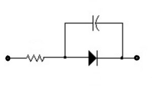
It turns out that the termination of the semiconductor crystal against a metal creates metal-induced gap states within the semiconductor’s band gap. The nature of these metal-induced gap states and their occupation by electrons tends to pin the center of the band gap to the Fermi level, an effect known as Fermi level pinning. A consequence is that it’s difficult to form ohmic contacts in semiconductors such as silicon and gallium arsenide. And the non-ohmic contacts arising from the phenomenon present a parasitic resistance to current flow that consumes energy.
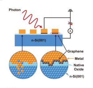
But future equivalent circuit models for Schottky diodes may not need the parasitic series resistance element thanks to work done at the Ulsan National Institute of Science and Technology in South Korea. There researchers have come up with a way to use a graphene layer to prevent an intermixing of materials at the semiconductor/metal interface, driven by the diffusion of metal and semiconductor atoms. Perhaps more important, the grapheme diffusion barrier has negligible electrical resistance that prevents materials from intermixing during thermal stressing.
Leave a Reply