
by Maniing Xie, System Application Engineer, Power Design Systems, Texas Instruments
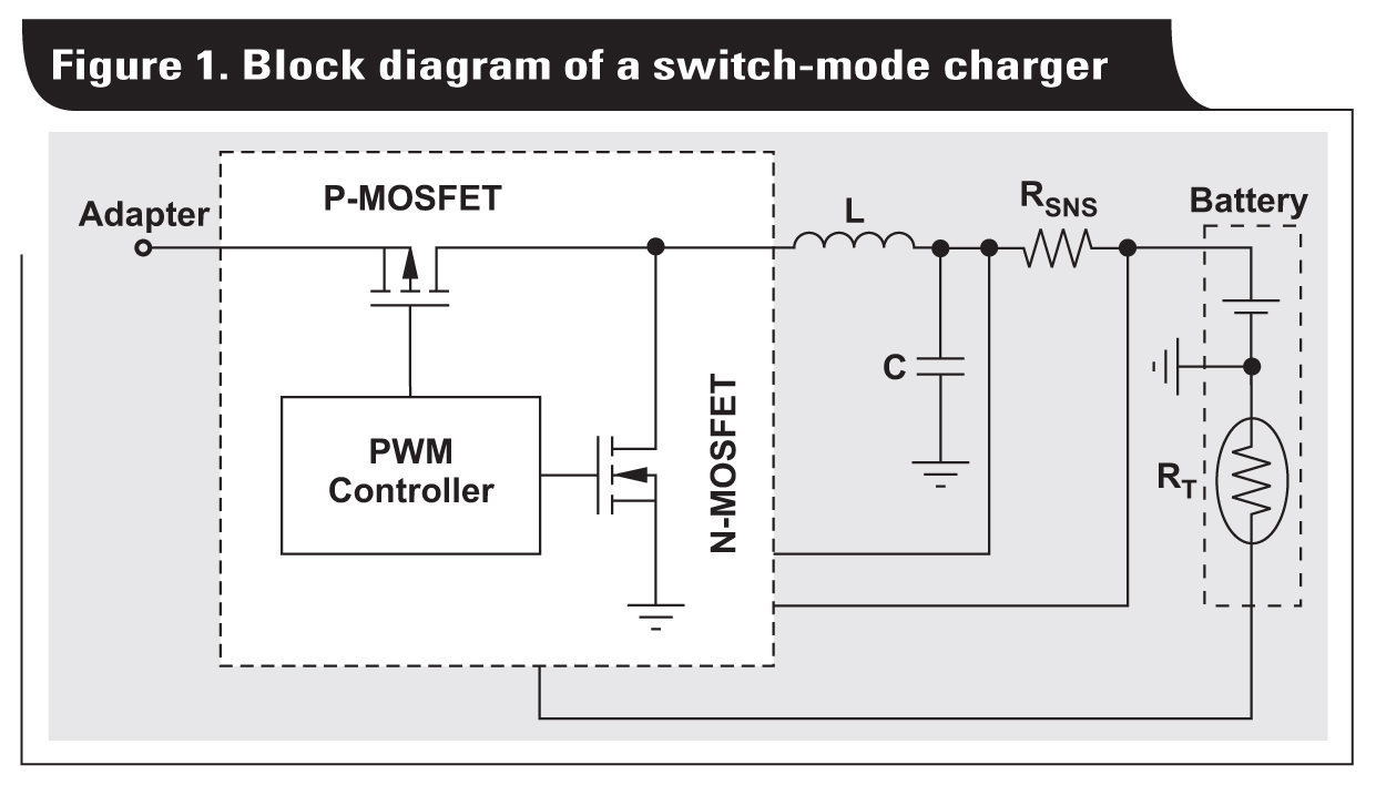
Electromagnetic interference (EMI) can create serious issues for manufacturers in an industrial environment. A buck converter generates a pulsating ripple current with high di/dt at the input. Without input capacitors, ripple current is supplied by the upper power source. Printed circuit board (PCB) resistance and inductance causes high-voltage ripple that disrupts electronic devices. The circulating ripple current results in increased conducted and radiated EMI. Input capacitors provide a short bypass path for ripple current and stabilize bus voltage during a transient event. In recent years, the advancements in power-MOSFET technology have dramatically increased switching frequency and gate driving speeds of switch-mode power supplies. Therefore, reducing the input-voltage ripple of a buck converter has become more challenging. This article uses a buck converter as an example to demonstrate how to select capacitors to achieve optimal performance. Figure 1 shows the basic circuit of a buck converter. The converter input current (iIN_D) consists of an alternating ripple current (ΔiIN_D) and DC current (IIN_DC).
Design parameters:
- Output voltage, VO = 1.2 V
- Maximum load current, IO = 6 A
- Estimated efficiency at maximum load, h = 87%
- Switching frequency, fSW = 600 kHz
- DC input bus voltage = 12 V with 5% tolerance
- Worst-case maximum input voltage, VIN_max = 16 V
- Bus converter control bandwidth = 6 kHz
- Transient load step, IStep = 3 A
- Worst-case board temperature = 75°C
Design requirements:
- Allowed input peak-to-peak ripple voltage, ΔVIN_PP ≤ 0.24 V
- Allowed input transient undershoot or overshoot, ΔVIN_Tran ≤ 0.36 V
The capacitor voltage rating should meet reliability and safety requirements. For this example, all input capacitors are rated at 25 V or above. The following discussion focuses on meeting electrical and thermal requirements, optimizing performance, and lowering size and cost.
- Select key ceramic capacitors to bypass input ripple current
Among the different types of capacitors, the multilayer ceramic capacitor (MLCC) is particularly good regarding allowable ripple current. A starting point is to select the key ceramic capacitors to meet the requirements for ripple voltage and current. Table 1 shows five different ceramic capacitors that were chosen for this article. Due to DC bias capacitance degrading, the effective capacitance is not the same as the rated capacitance.
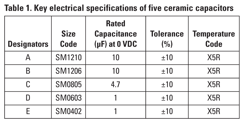
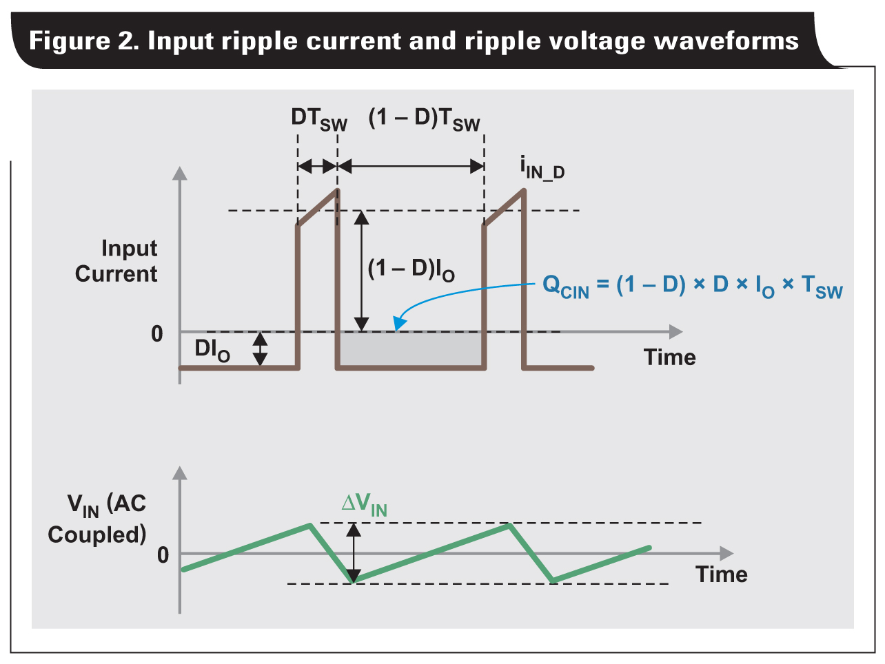
Figure 2 shows the AC current flowing through the input capacitors and the resulting voltage ripple across the ceramic capacitors, assuming the majority of the ripple current flows through these ceramic capacitors. Since the equivalent series resistance (ESR) of ceramic capacitors is very low, ripple resulting from ESR can be ignored.
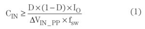
Equation 1 is used to estimate the required effective capacitance that will meet the ripple requirement. The worst case for this example occurs at maximum duty cycle, which is less than 50%.
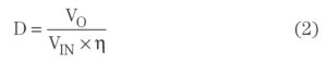
Duty cycle, D, can be calculated with Equation 2. For this example, D ranges from 8.6% to 12.1% with maximum load.
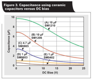
The input capacitance should be greater than 4.43 µF as calculated with Equation 1. Taking 10% tolerance into consideration, the total effective capacitance should be greater than 4.92 µF with 12-V DC bias. Figure 3 shows the effective capacitance over DC bias of different capacitors in the inventory.
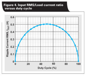
Besides the ripple-voltage requirement, the ceramic capacitors should meet the thermal stress requirement as well. A starting point is to estimate the maximum rootmean-square (RMS) of Δi IN_D. Figure 4 shows the ratio of input ripple current RMS over load current (IIN_RMS/ILoad) as a function of the duty cycle.
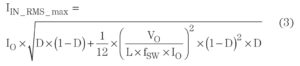
For this example, the maximum input ripple current RMS occurs at full load and with duty cycle of 12.1%, according to Figure 4. Now calculate IIN_RMS_max using Equation 3. IIN_RMS_max = 1.97 ARMS.
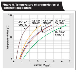
Since the board temperature is 75°C and the X5R MLCC is rated for 85°C, capacitor temperature rise should be lower than 10°C. Figure 5 shows the temperature rise characteristics of different ceramic capacitors.
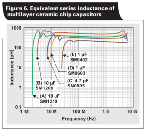
According to Figures 3 and 5, the ripple and thermal stress requirements can be met by combining two (B) capacitors or one (A) capacitor. Both selections have a similar cost and solution size. At this point, a third factor, the equivalent series inductance (ESL) should be included. Figure 6 shows the ESL of all five capacitors.
With two (B) capacitors in parallel, the combined ESL is about 0.3 nH, while one (A) capacitor has an ESL of 0.5 nH. Two (B) capacitors were selected for a total effective capacitance of 6 µF, and an allowable ripple current of 5.2 ARMS with a 10°C temperature rise.
2. Add small ceramic capacitor(s) with low ESL to alleviate input spikes and phase-node ringing
With MOSFET technology advancement, transition time is dramatically reduced which improves efficiency. This leads to a high di/dt slope of the input current and highvoltage spike at the input and phase node. The ESL of the ceramic capacitors plays a significant role. Thus, it is desirable to further lower the input capacitor ESL. This can be achieved by adding a small capacitor with low ESL. Despite the fact that ESL varies with material and structure, a common rule of thumb is that a capacitor with a smaller case has a lower ESL (Figure 6).
For phase-node ringing, it is common practice to use a boot resistor to slow down the gate speed and a snubber circuit for alleviation. However, both methods incur additional power loss and sacrifice efficiency. Phase-node ringing can be reduced without the penalty of lower efficiency.
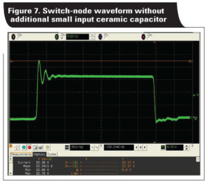
Figure 7 shows the phase-node waveform of the TPS53318 with two (B) capacitors as the only input capacitors. VIN is 16 V and the load is 6 A. The phase-node voltage spike is 22.7 V.
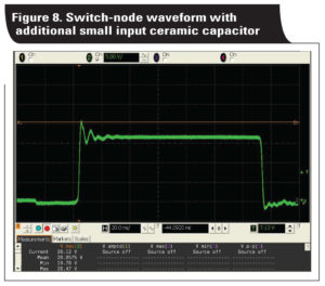
Under the same test conditions, one (D) capacitor was added to the input. As shown in Figure 8, the spike voltage was reduced from 22.7 V to 20.5 V. This is a significant improvement without sacrificing efficiency.
While an additional small ceramic capacitor can alleviate phase-node ringing, it can take up precious PCB space and in some cases increase cost. It is a trade-off of cost, size and performance. However, in this example, the added (D) capacitor did not increase the solution size.
3. Select bulk capacitors
While the MLCC is excellent regarding allowable ripple current, it is notorious regarding effective capacitance that is necessary to meet transient response requirements. Bulk capacitors with high capacitance are more cost-effective than using all ceramic capacitors. Aluminum electrolytic and polymer are popular capacitors for this purpose. There are two key factors for selecting bulk input capacitors: 1) overshoot and undershoot requirement of transient response; and 2) allowable ripple current requirement.
The ESR of the bulk capacitor (ESRB) and the capacitance (CB) need to meet the transient response requirement. Figure 9 shows the idealized load-transient current (iLoad), inductor current (iL), input-transient current (iIN_D) and bus-converter current (iPS). The average input current ( ἾIN_D) can be approximated by the product of iL and the duty cycle, D.
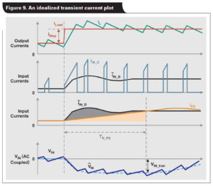
The ESRB should be lower than that calculated with Equation 4.
The second spike is related to the response of the bus converter. The converter output-current rise time during a transient event, TR_PS, can be approximated by Equation 5.

The capacitance of the bulk capacitor (CB) should be greater than that calculated with Equation 6.
Where CCE_Total is the total capacitance of the ceramic capacitors, and the tolerance of the capacitors is 10%. Also, CB should be greater than 15.07 µF. Given a 20% tolerance, the rated capacitance of the bulk capacitor should be greater than 18.84 µF.
Another factor for selecting a bulk capacitor is the allowable ripple current. It is a common practice that most low-cost electrolytic capacitors have an impedance that is much higher than the ceramic capacitors used for ripplecurrent bypassing. Thus, it can be assumed that the ripple voltage is not affected by the bulk capacitor. Figure 10 shows the idealized ripple current through the bulk capacitor.
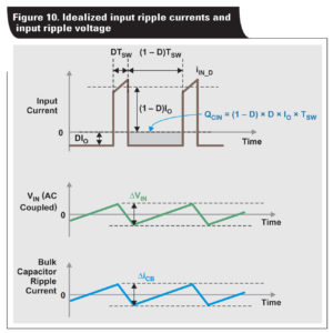
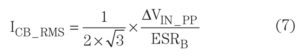
The bulk capacitor ripple current (ΔiCB) can be approximated by the input ripple voltage divided by the ESRB. Since the current-ripple waveform is triangular, the RMS of the ripple current (ICB_RMS) can be estimated with Equation 7.
The input ripple voltage can be calculated with Equation 8.
![]()
When selecting the bulk capacitor, ICB_RMS should be less than the allowable ripple current,
![]()
Thus, the allowable ripple current and bulk-capacitor ESR should meet the constraint specified with Equation 9 as shown by Equation 10.
![]()
With Dmax = 12.1%, CCE_Total = 6.6 µF and tolerance = 10%, the maximum input ripple voltage (ΔVIN_PP_max) is about 179 mV. Thus, the product of the allowable ripple current and the ESR should be greater than 51.7 mV by Equation 9. Table 2 shows the parameters of five different electrolytic capacitors.
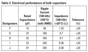
To meet both the transient and ripple current requirements, capacitor G was selected from Table 2 for the input bulk capacitor. For applications where one electrolytic capacitor is not sufficient, multiple electrolytic capacitors can be put in parallel to meet transient requirements.
However, the criterion for the product of the allowable ripple current and the ESRB remains the same. If no electrolytic capacitor meets the ripple-current requirement, extra ceramic capacitors are necessary. The extra ceramic capacitance can be estimated by solving Equations 8 and 9.
The proper PCB layout is also critical for the performance of the switch-mode converter. Robert Taylor demonstrated the recommended input capacitors placement in his Power Tips post.[1] Please refer to his blog post for input capacitor PCB layout recommendations.
The combination of ceramic and electrolytic capacitors renders a cost-effective solution for bypassing high-di/dt input ripple current and meeting load-transient response requirements. Following the tips and processes described could help you to select the proper input capacitors for a reliable, highly-efficient and compact DC/DC converter.
References
- Robert Taylor, “Don’t let your power supply layout ruin your day!” Power House blog, TI E2E™ Community, January 23, 2015.
- Chester Simpson, “Engineers Note: Capacitors are key to voltage regulator design,” (SNOA842), Texas Instruments, 2011.
Manjing Xie is a System Application Engineer, Power Design Systems at Texas Instruments, Inc.
What role the input inductor play or does not play in this discussion ?