
Silicon carbide and gallium nitride transistors both have their niche, but it pays to understand the applications in which each excels.
Zhongda Li, United Silicon Carbide Inc.
Wide band-gap (WBG) devices such as silicon carbide (SiC) and gallium nitride (GaN) are the hot topics of the moment, promising anything from universal wireless charging to power converters shrunk to almost no size. However, these are projections from theoretical performance that don’t always correspond with reality.
Let’s take a step back and just outline what WBG devices are. Semiconductors have bound electrons which occupy distinct levels around an atomic nucleus – valence and conduction bands. Electrons can move up to the conduction band and be available for current flow, but they require energy to do so. In WBG devices this energy requirement is much greater than with silicon. For example, SiC requires 3.2 electron-volts (eV) compared with silicon (Si) at 1.1 eV. The additional energy required to move WBG device electrons into the conduction band brings higher voltage breakdown performance compared with silicon of the same dimensional scale.
For the same reason, SiC can withstand higher temperatures (thermal energy) before failure and also, as a material, has a thermal conductivity about 3.5 times better than Si. In practice these attributes promise high temperature operation at high voltage and power levels.
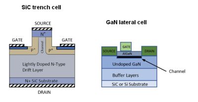
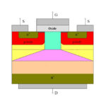
Devices initially available in SiC were simple diodes, but the material technology has advanced to allow fabrication of JFETs, MOSFETs and even bipolar transistors. Special geometric configurations used in the construction of SiC devices have brought additional advantages. For example, a SiC JFET with a vertical trench construction exhibits low ON-resistance compared with a GaN HEMT cell with lateral construction.
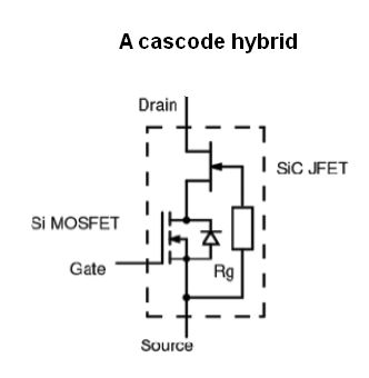
Although the devices are normally “ON” with zero gate voltage, a cascode arrangement of a co-packaged Si MOSFET with the SiC JFET gives a hybrid device with gate drive voltages compatible with Si MOSFETs that retains the advantages of WBG devices. (As a quick review, a cascode arrangement consists of a common-emitter stage feeding a common-base stage. The heavily loaded common-emitter stage has a gain of only one, overcoming the Miller effect. A cascode amp has a high gain, moderately high input impedance, and high output impedance, and a high bandwidth.)
Coming later than SiC, GaN has had slow adoption because of cost, yield, and reliability concerns. It is certainly theoretically capable of switching at higher speeds than SiC or Si, with its much higher electron mobility. But GaN thermal conductivity is lower than that of Si, so its power density potential is limited. Currently SiC devices are commonly used at around 650 V through 1.2 kV and higher, while GaN is limited to around 650 V where it struggles to compete with less expensive, more robust, and more mature SiC offerings at the same voltage.
GaN suppliers are targeting lower voltage/power markets that include data centers, EV/HEVs, and photovoltaics. However SiC also addresses these market areas, especially in applications for bi-directional dc-dc converters and totem pole PFCs. (As another quick review, a totem pole circuit uses one transistor to drive the output high, another connected below it to pull the output low. In totem pole PFCs, totem poles replace the four rectifier diodes to, among other things, eliminate the diode voltage drop.)
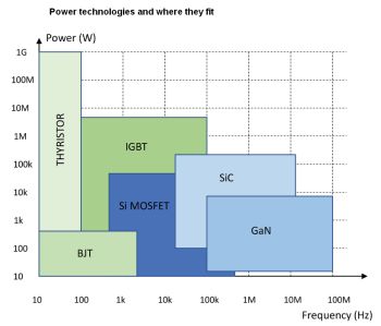
SiC addresses the IGBT market at high powers and voltages, and GaN targets the lower-power but higher-volume and cost-sensitive markets of Si MOSFETs. These applications all demand WBG benefits – potential higher efficiencies and smaller size, but inexpensive and reliable, and ideally second-sourced.
SiC is well established in the supply chain. SiC parts are available even from high-service distributors, whereas GaN parts have yet to become mainstream. The market analysis firm IHS Markit predicts this relative split in usage will remain into the mid-2020s, with the combined WBG market reaching $3.5B, of which GaN will represent only about $500M.
Even if GaN voltage ratings improve, SiC has an edge in industrial systems because it can withstand voltage avalanche conditions, as can happen with inductive loads. Manufacturers have extensive data showing SiC reliability in the prescence of voltage overstress. Makers of GaN devices make no claims except to say maximum voltage should not be exceeded.
A more tangible difference between SiC and GaN is the packaging; SiC parts are commonly available in TO-247 and T0-220 styles. Consequently, they can drop in as replacements for Si MOSFETs in existing designs. However, GaN device manufacturers recognize that plastic packages, with their inherent speed-limiting lead inductances, can be a barrier for performance. They have therefore mostly opted for surface-mount, single-source, chip-scale packaging, which limits their adoption in new designs. Here, the system design can take advantage of GaN device properties to make use of smaller passive components, particularly magnetics and capacitors.
Ironically, the real constraints imposed by meeting EMI standards and keeping dV/dt levels manageable often force designers to slow switching speeds with gate resistors. For example, dV/dt levels of 100 V/nsec are easily possible with SiC and GaN. But from I = C dV/dt, this dV/dt produces a 10-A current spike into just 100 pF of stray capacitance. Similarly, high di/dt values produce voltage spikes across connection inductance.
The state of the art
SiC devices are commonly available with 650-V and 1,200-V ratings at currents up to around 85 A with on-resistances of around 30 mΩ as cascodes as well as super cascodes – series-connected JFETs with ratings exceeding 3.5-kV. Single devices up to 1,700 V at around 70 A and 45 mΩ are available, but as MOSFETs rather than JFET cascodes. This means their internal body diode is relatively slow, unlike cascodes, and often must be bypassed with a costly fast external diode when the application requires it, as for example in bridge circuits.
GaN devices top out at 650 V with about a 60 A and 25 mΩ rating, equivalent to many SiC parts but theoretically capable of faster switching. Interestingly, today’s GaN devices with 100-V ratings are no better than traditional MOSFETs for on-resistance. So their speed advantage must be enough make it worth using GaN rather than commodity MOSFETs at this level.
IHS data predicts a significant rise in WBG device design-ins, although IGBT and traditional MOSFET sales are expected to also increase in a growing market. But there is a debate about how different WBG devices might dominate particular applications.
The high temperature capability of WBG devices with potentially fast switching and low losses makes them good candidates for military and industrial applications where performance is key. High-energy bridge circuits are obvious applications in inverters, welding equipment, class D audio amplifiers, motor drives, and more.
One application in particular that sees major benefits is the bridgeless
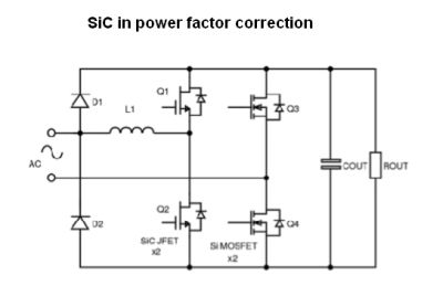
totem-pole PFC circuit. Here, versions using Si technology have been limited by the slow performance of body diodes in the MOSFETs. This slow response forces operation in a critical conduction mode, which in turn produces high peak currents and high EMI. But substituting cascode SiC JFETs allows operation in continuous-conduction mode. The result is better efficiency, smaller inductors, and fewer EMI problems. One such circuit at 1.5 kW, operating from a 230 Vac line, showed an impressive efficiency of 99.4%.
In high-power applications, operation in the presence of transient short-circuits and overvoltages is a major concern. A typical cascode SiC JFET has excellent qualities in this respect. High currents cause a pinch-off effect which limits current to a saturation level. Additionally, heating produced by the current reduces the channel conductivity, giving rise to self-limiting. The high allowed junction temperature also helps here.
For overvoltages, the SiC JFET gate-drain diode conducts, causing current flow in the gate drive circuit and turning the JFET channel on to clamp the overvoltage. Again, the inherent high temperature rating of the SiC die gives a good margin of safety for significant avalanche energy levels even in the relatively small die sizes encountered.
Manufacturers such as United Silicon Carbide Inc. have proven their SiC offerings are robust with parts qualified to 1,000 hours of operation biased into avalanche at 150°C. As an additional confidence measure, all parts go through 100% avalanche at final test.

In the statement “A typical cascode SiC JFET”
Is it really cascode or should it be cascade?
Cascode — https://www.analogictips.com/cascode-amplifiers/