
There are diode varieties which do much more than just block current flow in one direction and allow it in the other; some of these special diodes have favorable attributes while others are essential in modern electronics.
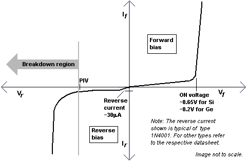
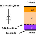
Every electronic engineer is familiar with the diode: it’s a basic, widely used, two-terminal semiconductor device. The diode’s basic function is simple: it blocks the flow of current in one direction (reverse bias), while allowing it in the other (forward bias), defined by the well-known V-I curve (Figure 1), and the equation describing behavior in the forward-bias region (Figure 2). Diodes are so critical, versatile, and needed that countless discrete versions are used throughout a circuit or embedded within an IC’s design.

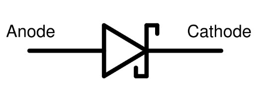
While the graph and equation apply to basic signal and power diodes, there are specialized variations of the basic diode that fulfill critical roles in circuits and systems. This FAQ will look at some of these signal and low-power diode types (excluding “power diodes” and LEDs) and their unique characteristics which make them useful in electronic designs. It will also show their most-common schematic symbols which are somewhat standardized (although there are many “local” variations due to regional difference and historical tradition).
Q: A little historical background, please: are solid-state diodes the only kind of diode?
A: No, not at all. The tiny quartz crystal-based diode was available by the late 1800s, but it could handle only minuscule amounts of power, was very finicky to build, and did not function reliably; it was viable primarily as a “detector” in crystal radios.
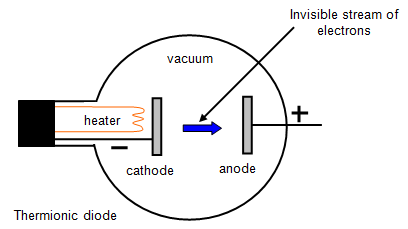
The first practical and reliable diode was the vacuum-tube Fleming diode, invented in 1904, also called the thermionic valve (Figure 3). This device allowed electrons (current) to flow only from cathode to anode (those terms are still used today!) and enabled conversion of AC signals and power to DC. By doing so, the Fleming diode set the stage for radically changing the world of “electricity” into electronics.
(This vacuum-tube diode was also the basis for the first active electronic device, the amplifying vacuum tube devised by Lee de Forest. It was the first step on the path to electronic systems as we know them. This triode vacuum tube had a grid interposed between the electron-emitting cathode and electron-receiving plate elements.)
Q: Seems like a lot of “work” (size, power, cost) for a simple rectifying function – was it worth it?
A: Yes, it was a lot of work, but it was worth it, as there was no alternative. However, by the 1930s, scientists discovered that the element selenium could be used for a power-rectifying function, and “solid state” selenium-based rectifiers were used in many cases to replace the vacuum-tube diode for AC/DC power conversion.
Q: That’s all interesting, but I want to hear about today’s semiconductor diodes. What are some specialty diodes in addition to basic small-signal diodes such as the classic IN914 or IN4001?
A: We will look briefly at these seven types: tunnel, Zener and avalanche, Schottky, varactor, Gunn, and PIN diodes. Each also has its own schematic symbol, which is derived from the standard-diode symbol.
Q: I never heard of the tunnel diode – what is it?
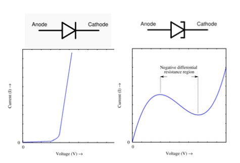
A: This diode, also called the Esaki diode after its inventor), was developed in 1957 by Leo Esaki and a team at the predecessor of Sony in Japan (he received the Nobel prize for this work). In brief, it has a “negative resistance” due to a quantum-mechanics effect called tunneling, where the voltage across the diode increases but the current through it decreases at a certain threshold (Figure 4).
Q: How does this happen?
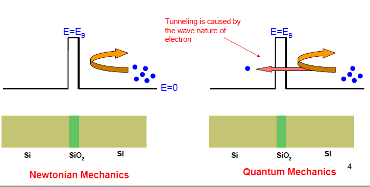
A: There is an energy barrier which electrons must cross at the P-N junction of any semiconductor diode. For a thick barrier, both Newtonian and quantum mechanics say that an electron can pass the barrier only if it has more energy than the energy-barrier “height.” However, for a very thin barrier, while Newtonian mechanics still says that the electrons cannot cross the barrier, instead quantum mechanics shows how the electron’s wave nature and wave function will allow it to tunnel through the barrier (Figure 5).
Q: We don’t hear much about the tunnel diode – what happened?
A: The tunnel diode was used as the core of high-frequency oscillators, and also for high-speed switching. But it never caught on in mass use, which is generally attributed to two reasons: advances in conventional semiconductor processes for those same applications made it unneeeded, and the practical difficulties of designing and controlling switching circuits using two-terminal devices, as their input and output “ports” use the same connections. (We’ll see this challenge again in part 2, with the Gunn and PIN diodes.)
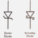
Q: What is a Zener diode?
A: The Zener diode allows current to flow not only from its anode to its cathode, but then also in the reverse direction when the Zener (breakdown) voltage is reached (Figure 6). It is named after Clarence Melvin Zener, who discovered the reverse-breakdown characteristic, again due to electron quantum-physics tunneling caused by a high-strength highly localized electric field (may seem the same but this is not the same as the tunnel diode physics).
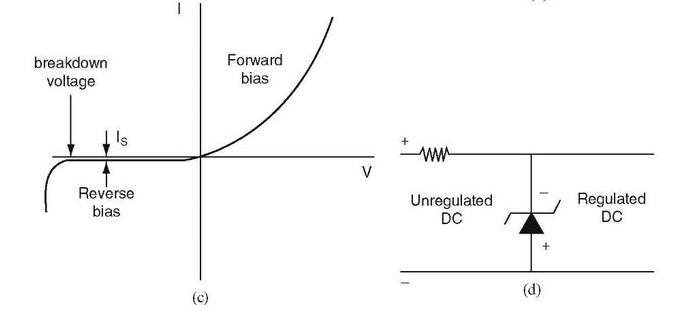
Note that many diodes described as “Zener” diodes rely instead on another physics mechanism called avalanche breakdown. Both breakdown types are used these reverse-breakdown diodes with the Zener effect predominating at lower voltages and avalanche breakdown at higher voltages. (Note that the Z in “Zener” is often spelled out as lower case ”zener.”)
Q: Where are Zener diodes used? Are they “defunct” as tunnel diodes are?
A: They are very much alive. Zener (and avalanche) diodes are used extensively for applications such as providing the reference voltage for power supplies and regulators. They are also used to protect circuits from overvoltage, such as from ESD. They can be manufactured to have specific breakdown voltages such as 1.5, 3.5, 5.0 V and other voltages, further increasing their usefulness, and are available as standalone discrete devices as well as being embedded in ICs for internal voltage references.
Q: I have heard of the Schottky diode; what does it do and how does it function?
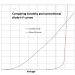
A: The Schottky diode (sometimes called a hot-carrier diode) (Figure 7), is named after the German physicist Walter H. Schottky and has the same V-I curve shape as a basic P-N diode. However, it has a much-lower forward-voltage drop of just 150 to 450 mV compared to a conventional silicon P-N diode forward-voltage drop of 600 to 800 mV. This lower forward voltage supports higher switching speeds and better system efficiency (lower drop means reduced IR and I2R losses) than those diodes.
The standard Schottky diode uses PN silicon but with a different doping scheme. This lower forward-voltage requirement allows higher switching speeds and better system efficiency, so it used for low-frequency circuits, switching power supplies, and RF circuits.
Part 2 of this FAQ will look at three other specialty diodes: the varactor, Gunn, and PIN diodes.
References
- Chennai Mathematical Institute (India), Ravitej Uppu, “V-I Characteristics of Diode”
- History-Computer, “The First Vacuum Tube”
- SchoolPhysics, “The thermionic diode”
- RF Café/Popular Electronics, “After Class: Working with Selenium Rectifiers”
- University of South Carolina, Department of Electrical Engineering, “Tunnel Diodes (Esaki Diode)”
- El-Pro-Cus, “Applications Involving in Zener Diode Working Functionality”
- Skyworks, “Varactor Diodes”
- Slideshare, “Varactor Diode”
- Electrical 4 U, “Gunn Diode”
- International Journal of Electrical and Computer Engineering (IJECE), “Miniature design of T-Shaped frequency Reconfigurable antenna for S-Band Application using Switching Technique”
- El-Pro-Cus, “PIN Diode Basics, Working and Applications”
- Microsemi/Microchip Technology Inc., “MicroNote Series 701: PIN Diode Fundamentals”
EE World Online References
- More options for SiC Schottky 1200-V diodes
- SPDT high-power PIN diode RF switches work up to 2.7 GHz
- What are diodes? A quick refresher
- What’s your type? Walk-thru of semiconductor diodes
- SPDT high-power PIN diode RF switches work up to 2.7 GHz
- SPDT PIN Diode Switches cover 10 MHz to 67 GHz range
- Gunn Diode oscillator operates at 24.125 GHz
- Meaning and measurement of negative resistance

Leave a Reply