
 YouTube has several videos featuring really bad designs for fast phone chargers. YouTubers doing these videos often point to problems such as transformers with chintzy insulation, line capacitors that lack the correct safety rating, and even chargers with plastic cases that heat up so much that they actually melt when there’s a heavy load.
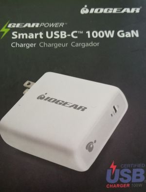
Fortunately, the charger we’ve torn down today doesn’t exhibit any of these unfortunate tendencies. In fact, it has proven to be a really good phone charger. It is a 100-W charger from IOGear made by Aten Technology in California.
Unlike some of the poorly conceived chargers in YouTube videos, the IOGear charger stays cool no matter what power level it is producing. As a bit of background, modern fast chargers typically can produce one of five output voltages—five, nine, twelve, 15, or 20 V—depending on what’s connected to them. The charger negotiates with the device under charge to decide which output voltage to supply.
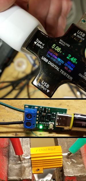
We simulated worst-case charging conditions with the IOGear charger using a dummy load and special testing gear designed specifically to exercise phone chargers. We ran the IOGear charger at its maximum power level for about a half hour and measured its case temperature. The charger ran nice and cool—its case temperature never got above room temperature. The half-hour charge time at full power is probably worst case, given the protocols used by fast chargers of this sort. Fast charging
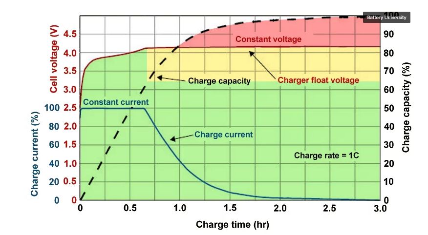
technologies exploit the constant current phase of a battery charge cycle by pumping as much current as possible into the battery before it reaches its peak voltage. Thus fast charging technologies are most effective—and handle the highest amount of power–when the battery is first plugged in and might be less than 50% full. The charger current automatically diminishes as the battery passes 80% capacity. So chargers see their worst-case maximum power handling scenarios in the first part of the charging process.

Once we removed the plastic outer case from the IOGear charger, the contrast between this high-quality charger and other less capable chargers starts to become clear.
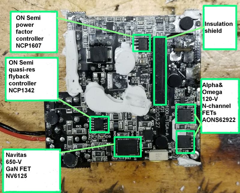
Cheap chargers have their circuitry pretty much exposed once the case comes off, but not the IOGear charger. Its circuit board is encased in a thick metal sub-enclosure that not only gives the charger some heft but also probably shields its circuitry and prevents radiation of EMI. Beneath the metal enclosure is a layer of insulating material. The charger circuit board itself includes potting material around the larger parts, apparently to help stave off failures due to vibration.
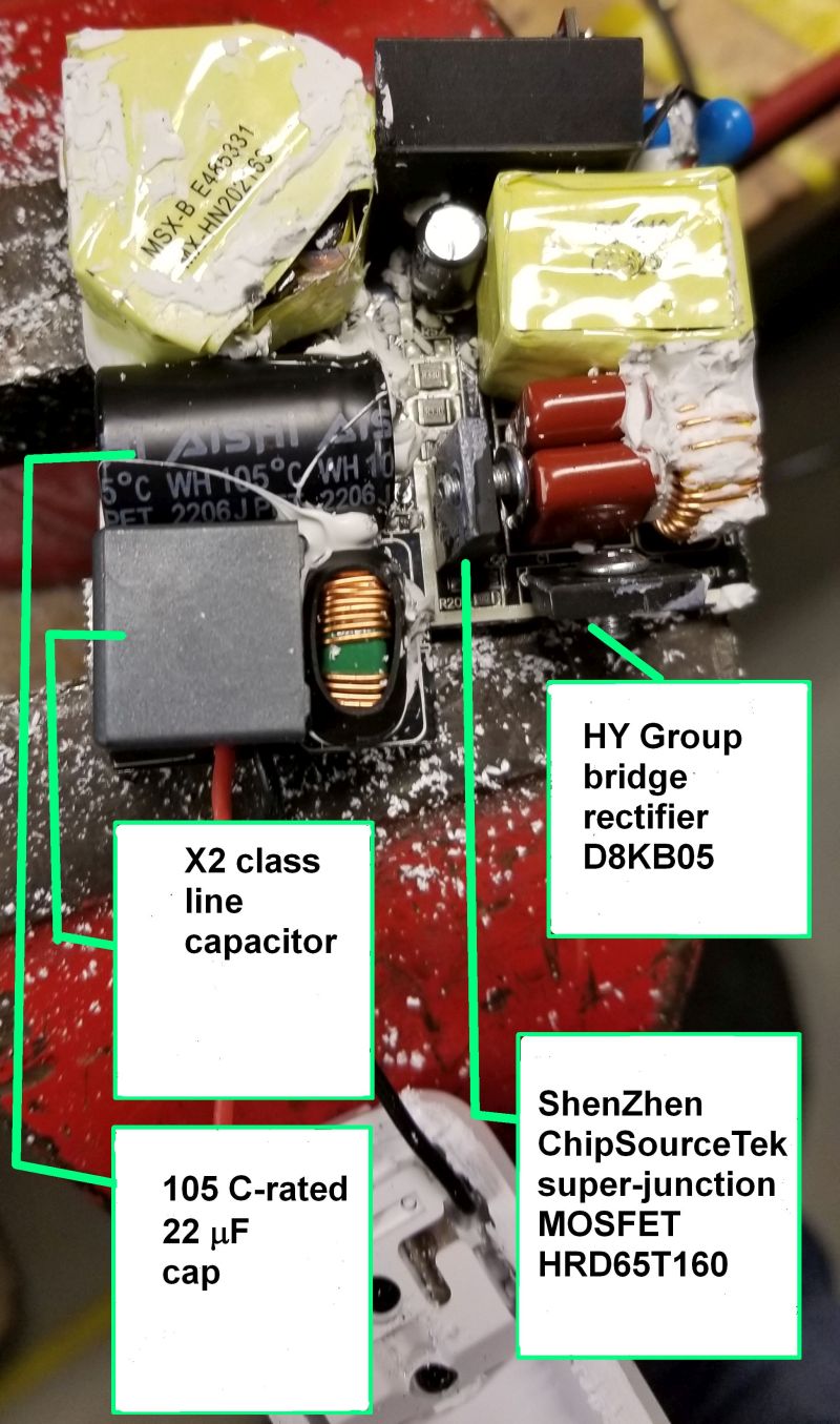
Poorly designed chargers often have cheap parts of questionable quality on their front end that connects directly to the ac outlet. That’s not what we found in the IOGear charger. It’s front end includes a beefy X2 subclass line-to-line capacitor as spelled out by the IEC 60384-14 safety standard which can withstand a 2.5-kV pulse. Also in the front end is a 220 μF electrolytic capacitor rated for 106°C. The capacitors work with a bridge rectifier from HY Electronic in Taiwan.
One noteworthy facet of the phone charger is that it incorporates both a power FET made from gallium-nitride and a super-junction power MOSFET made from silicon. Both are rated for 650 V. The super-junction MOSFET is from ShenZhen ChipSourceTek in China while the Gallium nitride FET is from Navitas.
It is interesting to compare the relative size of the gallium-nitride FET and the silicon super-junction FET. While both have 650-volt ratings, the super-junction transistor handles 21 amps to the gallium-nitride transistor’s eight. But though the silicon transistor handles a bit more than two and a half times as much current as the gallium-nitride device, its package takes up almost 14 times more volume. Which helps explain one of the reasons switching supplies like this one increasingly use wide bandgap semiconductors like gallium nitride.
The Navitas gallium nitride FET seems to be the main power transistor for sending charging current to the load. The super-junction MOSFET, judging by its position on
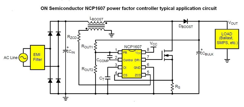
the circuit board, might play a role in power factor control. The power factor control itself is handled by an ON Semiconductor chip. It uses a Critical Conduction Mode technique where a power switch turns on immediately when current in an inductor drops to zero.
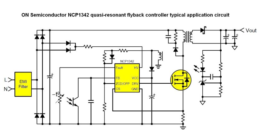
The charger uses a quasi-resonant flyback switching topology. As a brief review of what goes on, a key feature of quasi-resonant converters is that the turn-on and turn-off of the power transistor happens at zero current and voltage, resulting in an essentially lossless switch action. The claim to fame of Quasi-resonant switching, also known as valley switching, is that it reduces the EMI the power supply produces thanks to its soft switching action. And switching when a voltage and current valley is detected, rather than at a fixed frequency, introduces a natural frequency jitter that spreads the RF emissions spectrum.
The chip that handles the quasi-resonant flyback control in this charger is another ON Semiconductor device that also incorporates features for minimizing power consumption under a light load.
Rounding out the main components on the IOGear circuit board is an N-channel FET from Alpha&Omega Semiconductor that may be part of the PWM generation.


hi i want to learn about such qc+pd chargers . i want to learn detail explanation of each component used and its use. schematic diagram explanation and circuit diagram