• Skip to primary navigation
  • Skip to main content
  • Skip to primary sidebar
  • Skip to footer
  • Subscribe
  • Advertise

Power Electronic Tips

Power Electronic News, Editorial, Video and Resources

  • Products
    • Power Supplies
    • AC-DC
    • DC-DC
    • Battery Management
    • Capacitors
    • Magnetics
    • MOSFETS
    • Power Management
    • RF Power
    • Resistors
    • Transformers
    • Transistors
  • Applications
    • 5G
    • AI
    • Automotive
    • EV Engineering
    • LED Lighting
    • Industrial
    • IoT
    • Wireless
  • Learn
    • eBooks / Tech Tips
    • EE Training Days
    • FAQ
    • Learning Center
    • Tech Toolboxes
    • Webinars & Digital Events
  • Resources
    • Design Guide Library
    • Digital Issues
    • Engineering Diversity & Inclusion
    • LEAP Awards
    • Podcasts
    • White Papers
  • Video
    • EE Videos & Interviews
    • Teardown Videos
  • EE Forums
    • EDABoard.com
    • Electro-Tech-Online.com
  • Engineeering Training Days
  • Newsetter Subscription

Technical papers demonstrate 15 V and 650 V GaN power device performance and reliability data

May 20, 2022 By Aimee Kalnoskas Leave a Comment

Innoscience Technology will present two papers at the prestigious IEEE International Symposium on Power Semiconductor Devices (ISPSD) conference in Vancouver, Canada, May 22-25.

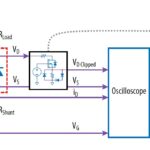
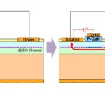
The first paper systematically evaluates the reliability and switching lifetime of a 650-V commercial GaN-on-Si HEMT fabricated on a 200mm (8-inch) CMOS-compatible process platform for a high-density PFC Boost power converter application. Innoscience’s engineers shows that by adopting Innoscience’s Strain Enhancement Layer (SEL)technology, a stable Dynamic RDS(on) (< 1.2x) during the 1000-hrs switching stress test is achieved, which is further confirmed by the wafer-level stress system. Device without SEL layer, on the contrary, shows a quicker degradation of the Dynamic RDS(on) that increases 18 times during the first 3 hours of stress. By performing Emission Microscope (EMMI) to detect the electroluminescence of device in situ during switching stress, scientists at Innoscience has highlighted that the SEL suppressed the hot carrier injection, which is believed to contribute to the increase of the Dynamic RDS(on) on samples without SEL technology.

Hot carrier photoemission for device w/o SEL (a) 350 V, (b) 500 V, and w/ SEL (c) 350 V, (d) 500 V. (e) Device cross-section shows the hot carrier location and photoemission.


Comparison of dRon without and with the SEL under the hard switching test with Vds = 600 V, Vgs = 6 V, and fs = 100 kHz.

The second paper is titled ‘Dynamic RDS(on) and Vth free 15 V E-mode GaN HEMT delivering low switching Figure of Merit (sFOM) of 13.1 mΩ·nC and over’. The power devices discussed achieve record-low sFOM on commercialized 200 mm GaN-on-Si platform made for mass production. Although tremendous efforts have been made in low voltage GaN HEMT for consumer electronics, where power switches are typically below 40 V, the wide adoption of low voltage GaN HEMT still faces huge challenge as compared with its silicon counterpart as the contact resistance or parasitic capacitance proportion rises up as dimensions shrink down, the threshold voltage Vth decreases and the risk of false turn-on increases, off-state leakage current increases and results in large quiescent loss and long-term static and dynamic instability. All these issues hinder the wide acceptance of low voltage GaN HEMT in volume constrained portable electronics.

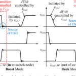
Innoscience shows that their InnoGaN withstands 1000 hours’ continual stress over wide temperature range with minimum parametric shift and continuous-switching stress in both hard-/soft-switching mode with negligible dynamic Ron and Vth shift. Device performance is further validated in buck converter with GaN HEMTs in half bridge configuration and demonstrates superior efficiency over 80% at tens of MHz. Thus, InnoGaN HEMTs rated for 15V unlocks the full potential of GaN power switches targeting for fast-speed high-frequency buck converter in tens of MHz with peak efficiency 90% with long-term system dynamic stability.

(a) Optical microscopy of the 15 V GaN HEMT in wafer-level chip-scale package (WLCSP) with few pH parasitic inductance. (b) Cross-section of the fabricated GaN HEMT.

Dr Denis Marcon, General Manager, Innoscience Europe comments: “The two papers are highly detailed and include comprehensive test data as befits submissions to this industry-recognized, important IEEE conference. We hope that attendees will understand that Innoscience is clearly the leader in GaN devices produced on 8-inch silicon wafers, with fully-characterised performance and reliability data both for Low Voltage (LV) and High Voltage (HV) devices.”

You may also like:


  • Is Double Pulse Testing inadequate for GaN devices?

  • How reliable are GaN HEMTs?

  • What is d-GaN, e-GaN and v-GaN power?
  • GaN power devices
    GaN power devices, Part 2: application
  • GaN power devices
    GaN power devices, Part 1: principles

Filed Under: Power Supply News, Transistors Tagged With: innoscience

Reader Interactions

Leave a Reply

You must be logged in to post a comment.

This site uses Akismet to reduce spam. Learn how your comment data is processed.

Primary Sidebar

Featured Contributions

Vertical power delivery reduces losses in AI processor designs

Protecting Ethernet interfaces in telecommunications applications against common high energy surges

Ionic cooling: a silent revolution in thermal management

Robust design for Variable Frequency Drives and starters

Meeting demand for hidden wearables via Schottky rectifiers

More Featured Contributions

EE LEARNING CENTER

EE Learning Center

EE TECH TOOLBOX

“ee
Tech Toolbox: Aerospace & Defense
This Tech Toolbox dives into the technical realities of modern defense, exploring how MBSE is streamlining aerospace design and what’s next for radar and electronic warfare.

EE ENGINEERING TRAINING DAYS

engineering
“power
EXPAND YOUR KNOWLEDGE AND STAY CONNECTED
Get the latest info on technologies, tools and strategies for EE professionals.
“bills

RSS Current EDABoard.com discussions

RSS Current Electro-Tech-Online.com Discussions

  • Bot checks
  • timing delay code statements using Swordfish
  • S1MJ ?
  • Getting into an LED bulb
  • Understanding reversing polarity at astable multivibrator

Footer

EE World Online Network

  • 5G Technology World
  • EE World Online
  • Engineers Garage
  • Analog IC Tips
  • Battery Power Tips
  • Connector Tips
  • EDA Board Forums
  • Electro Tech Online Forums
  • EV Engineering
  • Microcontroller Tips
  • Sensor Tips
  • Test and Measurement Tips

Power Electronic Tips

  • Subscribe to our newsletter
  • Advertise with us
  • Contact us
  • About us

Copyright © 2026 · WTWH Media LLC and its licensors. All rights reserved.
The material on this site may not be reproduced, distributed, transmitted, cached or otherwise used, except with the prior written permission of WTWH Media.

Privacy Policy