
New silicon-carbide FETs perform better than previous versions and can replace silicon MOSFETs with relative ease.
Anup Bhalla, VP Engineering UnitedSiC
Wide-bandgap (WBG) semiconductors are now accepted as the future of high-efficiency power conversion. The reason: they provide lower conduction and switching losses than otherwise-comparable silicon-based IGBTs or MOSFETs. Since the introduction of WBG silicon carbide (SiC) JFETs in 2008 and SiC MOSFETs in 2011, yield, performance and costs have all improved such that it is reasonable to say overall system cost with SiC is lower than that of silicon, if benefits are fully exploited.

Some inconveniences have remained though. SiC JFETs are normally-on devices, and SiC MOSFETs require particular gate drive conditions for best performance. The situation is different, however, for SiC FETS. These devices are formed from a cascode arrangement of a SiC JFET and low-voltage silicon MOSFET. They address the inconveniences of conventional SiC devices and exhibit lower losses.
Generation-three SiC FETS excel in relatively high-power applications. Low-loss 650-V, 1,200-V and 1,700-V parts are becoming key enablers for high-efficiency power conversion in EVs, chargers, alternative energy, circuit protection and IT infrastructure. Gen-3 SiC FETs can displace IGBTs and the best of the available silicon ‘Super-junction’ MOSFETs at these voltage levels. Even higher voltage ratings can be realized with stacked arrangements, and higher currents are possible when devices are paralleled. Gen-3 SiC FETs now provide lowest-in-class RDS(ON) figures for 650-V and 1,200-V devices, at less than 7 mΩ and 9 mΩ, respectively.
Development of SiC FET technology has continued beyond Gen 3, driven by the need for higher efficiency and power density, along with better thermal and electrical design margins. These goals can be realized by further reducing conduction and switching losses, but designers also want to see lower costs without a compromise in quality.
Responding to such demands, latest-generation SiC FETs have better specifications. These Generation 4 SiC FETs are rated at 750 V, a significant operating voltage margin over 650-V SiC MOSFETs. Power conversion efficiency improvements arise from advanced wafer-thinning and cell density maximization processes that improve the Figure Of Merit (FoM) of on-resistance/unit die area (RDS.A). This FoM combines a measure of static and dynamic losses stemming from the die size. It includes associated device capacitances and effects of reverse recovery charge Qrr. A low RDS.A value implies a high yield from wafers and potentially lower costs. In practice, the low absolute value of on-resistance doesn’t compromise current ratings. The high thermal conductivity SiC substrate and an advanced silver-sintered die-attach technique combine to provide good heat transfer. These benefits come without losing the easy 0-12-V gate drive characteristic of SiC FETs.
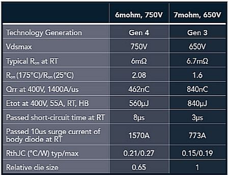
Gen 3/Gen 4 comparison
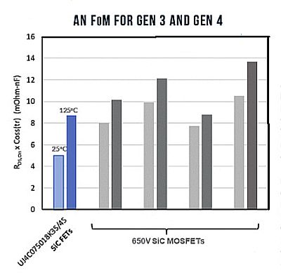
Parameters that directly affect efficiency for a SiC FET device, such as RDS(ON), Qrr and EOSS, are all significantly better with the RDS.A FoM of Gen
4. Gen 4 devices show a higher rate of increase of on-resistance with temperature, but this effect is swamped out by overall efficiency improvements compared with alternative technologies such as SiC MOSFETs. Moreover, Gen 4 devices exhibit more than double the short-circuit withstand time from 3 µsec to 8 µsec. Body diode surge current withstand is also about double at 1,570 A for the devices considered.
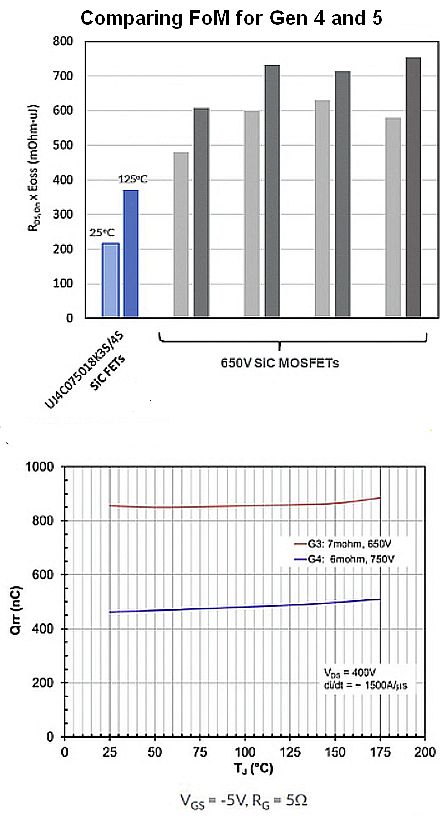
Another FoM, RDS(ON)×EOSS, is also a useful measure in hard-switching applications such as a Totem Pole PFC stage or a standard two-level inverter. In these circuits, device output capacitance COSS discharges rapidly from a high voltage, producing potentially high transient power dissipation. Gen 4 devices can be designed to keep COSS and resultant stored energy EOSS low, but typically at the expense of die on-resistance and consequent conduction loss. So the FoM RDS(ON)×EOSS captures the compromise.
In hard-switching applications, it is important to keep reverse-recovery energy in any body diode effect low to maintain high efficiency. This energy varies at a low rate with temperature in Gen 4 devices.
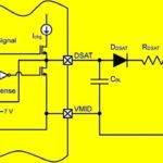
When devices are in reverse or “third quadrant” conduction, voltage drop is important as well. In SiC FETs the value is lower than with SiC MOSFETs. In a SiC FET, the drop is the sum of the JFET channel voltage, conducting in reverse at around 1.3 V, and the “knee” voltage of the body diode of the co-packaged Si MOSFET. Because the Si MOSFET is a low-voltage type, knee voltage is around 0.7 V, making the total 2 V. The comparable figure in a SiC MOSFET is around 3 to 5 V, so the MOSFET would dissipate proportionally more energy.
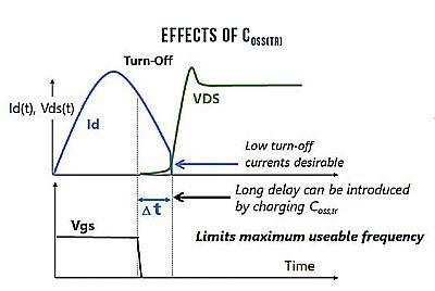
Soft-switching applications such as LLC and PSFB converters also benefit from use of SiC FETs. Peak currents can be high in these circuits, and the low RDSON value keeps conduction losses low. Additionally, the low output capacitance COSS(tr) value of SiC FETs enables the use of higher switching frequencies because of the shorter switch turn-off delay.
It is important in many applications to maximize switching frequency to get the ancillary benefits of smaller passive components, particularly magnetics. A useful FoM for soft-switching performance is
RDS(ON)×COSS(tr). A typical SiC FET compares well with otherwise-comparable SiC MOSFETs in this metric.
Gen 4 SiC FETs clearly have an efficiency edge over comparable SiC MOSFETs, but not at the expense of ease-of-use. The latest generation parts can still be driven effectively with a 0-12-V gate signal at a maximum of ±20 V, with ESD clamp diodes incorporated. The gate threshold is around 5 V and is nominally temperature independent, unlike in SiC MOSFETs.
The level of SiC FET gate drives is compatible with that for traditional Si MOSFETs or IGBTs, simplifying the task of retrofitting SiC FETs into older designs for a boost in performance. If designers optimize gate resistors and reduce snubbers in these legacy designs, swapping in SiC FETs can yield even higher efficiencies and lower costs. Even the losses in the SiC FET gate drive circuit are substantially lower, dropping from what can be watts in an IGBT circuit to near zero. Unlike in the older switch technologies, SiC FETs effectively have no Miller effect, which avoids problems of phantom turn-on as drain voltage rises. Similarly, SiC FETs are available with a Kelvin source connection which prevents source package connection inductance from interacting with the gate-drive loop, producing a similar unwanted spurious turn-on effect.
With the prospect of better efficiency, higher power density and lower system costs, 750-V Gen 4 SiC FETs are a compelling choice for applications with 400 or 500-V bus voltages. They provide an enhanced margin over commonly used 650-V-rated devices in other technologies. Standardized packaging with Kelvin connection options and an advanced thermal design make the parts easy to implement into new and legacy power conversion products in traditional and emerging applications.


Leave a Reply