
by Leland Teschler, Executive Editor
A big effort is underway in the U.S. to develop the kind of manufacturing expertise necessary to cheaply produce electronic circuits able to bend and flex.
The idea of putting electronic circuits on pieces of plastic that can bend certainly has a lot of sex appeal. And no wonder. The developments in this kind of flexible electronics already make headlines and promise even more excitement in the near future.
As an example of what’s possible today, consider a full-color liquid crystal display recently shown at a trade show by a firm called FlexEnable. The 4.7-in. display could bend into a cylinder having a radius of about 1.18 in. It also was made on relatively inexpensive plastic known as TAC (triallyl cyanurate), which is commonly used for display polarizer sheets.
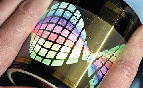
There’s only one problem with this accomplishment, at least if you reside in the U.S.: FlexEnable is a firm in the U.K. A lot of the work done in flexible electronics now takes place outside U.S. borders, thanks partly to programs sponsored by foreign governments. The FlexEnable displays, for instance, are part of a program called the Printable Organic Semiconductors for Highly Enhanced Displays, sponsored by the U.K. government. The firm collaborated with entities that include the Imperial College London and the University of Cambridge to get the kind of film uniformity needed for large-area, flat-panel displays.
“Europe and parts of Asia are heavily investing in flexible and hybrid-flexible electronics. We are behind,” said Mark Poliks, a professor at Binghamton University in New York and director of the Center for Advanced Microelectronics Manufacturing (CAMM) there. “As usual, we have invented and enabled many of these things, but we are not pushing the development end.”

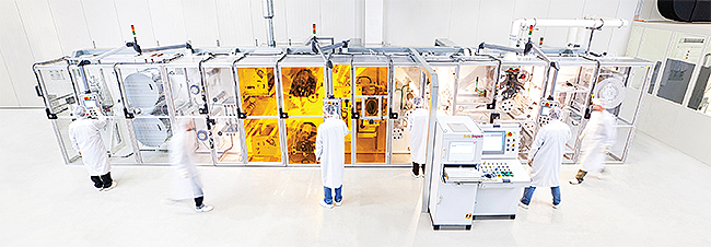
CAMM is part of an effort called the FlexTech Alliance (formerly the U.S. Display Consortium) targeting flexible electronics. Binghamton University focuses on developing next-generation roll-to-roll (R2R) electronics manufacturing capabilities—basically, processing circuit substrates in a manner analogous to printing newspapers on web presses. It further concentrates on what’s called flexible hybrid electronics (FHE) that combines the manufacturing integration of electronic components, such as silicon CMOS, and the direct manufacturing of electronics on flexible substrates. In that role, it has acquired prototype tools and established processes for producing low-volume items that serve as test-beds for new ideas.
CAMM isn’t the only U.S. facility to focus on flex. A new flex electronics research facility called NextFlex, for the Flexible Hybrid Electronics Manufacturing Innovation Institute, is being set up in Silicon Valley and will be run by the FlexTech Alliance, a San Jose-based public-private consortium. Over the next five years, the U.S. DOD will fund it with $75M through the Air Force Research Laboratory. 96 organizations—including companies, R&D labs and universities—pledged to add $90M more.
The DOD funding comes because the military is interested in flexible electronics as an innovation technology capable of slashing the size and power consumption of devices that troops carry. The average Marine today carries an “assault load” of up to 130 lb, whereas the recommended load is 50 lb. And the DOD increasingly puts wearable technology on military personnel. One application in the works could be a smart patch capable of monitoring a war-fighter’s physical and cognitive functions.
It’s also thought the Army Iron Man exoskeleton could be built significantly lighter thanks to flex electronics. Similarly, avionics could be made lighter and in complex shapes that can conform to airplane wings.
However, funding from the likes of the FlexTech Alliance isn’t just a government handout. “When we work with companies, we typically form a consortium that gives insight into the research and development issues being funded,” said FlexTech Alliance CEO Mike Ciesinski. “We periodically issue requests for proposals. The winners must match the funding award with the same amount or more of their own resources. For a dollar of R&D funding, the U.S. government pays for only about $0.35 of it. Private industry picks up the rest. NextFlex will adopt this same model and refine it.”
Examples of companies engaged in flexible electronics include a firm called Heliatek. It makes multilayer solar cells that use organic materials on PET film as a means of absorbing both visible and infrared light in active layers that are only about 250 nm thick. The solar cells, called HeliaFilm, are made using vacuum deposition in an R2R process.

FlexTech Alliance member ThinFilm was the first to commercialize printed, rewritable memory. The company is creating printed systems that include memory, sensors, displays and wireless communications. ThinFilm’s first product was a printed memory tag that uses a ferroelectric polymer to provide non-volatile, fully rewritable data on a label. The memory is produced with an R2R printing process using thin, inexpensive plastic (PET or PEN) substrate. The ferroelectric polymer is printed between layers of printed electrodes. Two protective coatings complete the fabrication. ThinFilm also says it recently completed a successful trial run of R2R printed displays.
Imprint Energy, also a FlexTech Alliance member, is developing printed, flexible rechargeable batteries based on zinc chemistry. Called Zinc Poly battery technology, the devices are said to be scalable to large dimensions for sheet or web-processing. The company thinks its batteries will be competitive with lithium-polymer cells but at less than half the cost and without the safety issues. Zinc forms the anode part of the battery, the cathode is a metal oxide, and the electrolyte is a solid material. Ordinarily, it is tough to make a zinc battery that is rechargeable because zinc usually forms dendrites, tiny fibers that grow and impede the charging reaction. The use of a special solid electrolyte is said to solve this problem.
Additionally, use of zinc minimizes the need for special packaging because zinc doesn’t react much with the environment. Zinc Poly batteries can also be just a few hundred microns thick (the width of a couple human hairs) and can be manufactured using thick-film deposition equipment such as screen printers.
Research areas
The usual approach for flexible electronics makers has been to adopt manufacturing equipment originally designed both for handling rolls of packaging material and for traditional semiconductor chips. “At CAMM, we use a lot of equipment from packaging and conversion world and extend it to work with embossing or vacuum deposition for patterning circuits,” said Poliks. “To some degree we are merging equipment from the packaging, conversion and display industries for large area and thin film devices and wiring. And we are adapting what was done for the back end of semiconductor wafers on the single-micron scale so it can work on larger areas and on non-traditional substrates.”<
One of the trickiest parts of making flexible electronics is in the precise patterning of circuit features. Patterning in traditional R2R products often isn’t critical; when magazines and newspapers come off roll presses with their images misregistered, the result is annoying but not catastrophic. But a few misregistered features on an R2R circuit are likely to make the whole device nonfunctional. So researchers have come up with numerous schemes to keep circuit patterns lined up.
“To make micron-sized features, you have to frame and immobilize the substrate so it is flat,” said Poliks. “Some approaches use advanced adhesives to glue down a polyethylene film on a glass subcarrier, then run that sandwich through all the processes. The drawback is in ensuring you don’t exceed the debond temperature or do something that will make the plastic lift off the glass surface. Another approach is to frame the material so it is free standing but held tight like a drum in all directions on the frame. Then the framed substrate travels through the process. But the approach we often use at CAMM is to convey the substrate without any framing. The tool itself is built into it a stage or drum that supports the plastic or glass to keep it flat and stable for processing.”
The kinds of patterning such techniques make possible is beginning to approach that of conventional integrated circuits. “There are companies making flex circuits using R2R that can get line widths on the order of 25 microns,” said Poliks. “Features on the order of one micron are also possible in R2R, but you still need photolithographic processes to do it. Additive circuit printing processes are getting better, but the inks tend to be too resistive. For smaller features you need metal-like conductivity that only comes with IC patterning and processing methods.”

Patterning challenges
One of the IC patterning methods Poliks refers to is vacuum deposition and particularly vacuum-deposition of metal layers. The deposited layers can range from the thickness of an atom up to millimeters. Deposition takes place at pressures well below that of atmospheric pressure as a way of both reducing contaminants in the deposition chamber and controlling the composition of the deposited material. But there can be difficulties in vacuum-depositing materials on flexible plastic substrates.
“In vacuum deposition, the traditional perspective is that plastics out-gas a large amount of low-molecular-weight molecules,” said Poliks. “Our first vacuum deposition tool had a large pumping capability and big chillers to affix anything out-gassed from plastic webs so we could get reasonable performance. But surprisingly, we have not had problems dealing with out-gassing. We are able to work at reasonable pressures, make sputtered dielectrics that use silicon and a small doping of aluminum to make oxides suitable for active devices, dielectrics and insulators.”
Another potential problem is that plastic substrates can absorb a small amount of moisture. The difficulty here is that many of the processing steps for depositing and patterning circuit materials use chemicals mixed with water, etching and stripping the plastic substrate with aqueous fluids at various points in the patterning process.
“Most of the concerns about plastics absorbing water center on soldering and reflow and storage conditions,” said Poliks. “We haven’t really had a problem with these so far because we haven’t required those kinds of processes. The substrate doesn’t sit in water, but there is a potential for moisture absorption because the substrates are thin. It’s important to understand the sequence of the process, be aware of where bakes take place, and precede soldering with an appropriate bake to head off moisture problems.”
The alternative to managing the potential for plastic out-gassing and moisture problems is to use a different kind of substrate: flexible glass. In recent years, manufacturers such as Corning have developed varieties of glass that are only 100 µm thick. Corning’s Willow glass, about as thick as a sheet of paper, was developed for smartphone displays but is flexible enough to come in rolls and be processed R2R equipment.
“Use of thin, flexible glass for flex electronics is like someone saying you can get a silicon substrate on a roll,” said Poliks. “The surface is capable of high-temperature processing, and flexible glass will be made in high volumes in the future. So high-end flex electronics will probably be fabricated on thin glass, mid-range on plastics. When you can tolerate the resistances available in 3D-printed circuits, we’ll probably see circuits on paper substrates for disposable and biodegradable applications.”
Corning Willow Glass differs from the more widely known Gorilla Glass. Willow Glass is an alkali-free glass composition manufactured in thicknesses between 100 to 200 µm and wound continuously onto a spool. This reduced thickness enables thin, lightweight and conformable flexible electronic devices. Where Gorilla Glass uses chemical-strengthening, ion-exchange methods to get the mechanical durability for portable cover glass, Willow Glass is not chemically strengthened.
Another reason glass makes a good substrate for flexible electronics is the smoothness of its surface. Substrate surface quality can affect factors such as electronic device yield and performance. Willow Glass, for example, requires no secondary polishing (or planarization) for advanced coating, display and electronic applications. The low surface roughness enables fabrication of TFTs, OLEDs and other thin-film electronic structures with no pinhole or shunt defects. In contrast, most plastic substrates used for electronic substrates need some sort of planarization layer to get the necessary smoothness. And glass has natural moisture and oxygen barrier properties that are difficult to replicate with plastic substrates.
It also looks as though flexible glass substrate material will have enough applications to be manufactured in high volumes, keeping prices down. Corning sees its Willow Glass being used in touch panels and displays for smartphones and tablets, and is actively pursuing applications in OLED lighting and PV with flexible/conformable devices for these applications in mind.
Research topics
There is still much work to be done in perfecting flex circuit elements. Thin-film transistors (TFTs), for example, now drive liquid-crystal displays and hold promise for new applications in flexible electronics. Commercial display applications mostly use hydrogenated amorphous silicon (a-Si:H) TFTs. One problem is that the nature of the charge transport in organic semiconductors and the microscopic origin of charge carrier traps isn’t well understood. Traps dominate transport in a-Si:H. Consequently, the field effect is about 1,000x lower in organics than in single-crystal silicon. And the field effect is what FETs depend on to modulate the current they pass. So getting a handle on these charge transport mechanisms is a research topic.
There are also efforts aimed to getting the kind of high performance out of flex circuits that is normally available only from CMOS devices, which are fabricated using harsh high-temperature processes that damage most flexible materials. On this front, recently a team led by France’s Institut d’Electronique de Microélectronique et de Nanotechnologie developed a way of building radio-frequency CMOS circuits on a variety of flexible substrates: polyimide plastic film, glass and stainless steel. The group first built RF CMOS circuits on a silicon-on-insulator substrate, then thinned it to 30 µm by completely removing the backside. They then transferred the circuits to flex substrates using a laminating process. The circuitry was attached to plastic and glass substrates by laminating it using a dry polymer film and rollers. The researchers say their technique can be adapted for ultra-mechanical flexibility, heat dissipation and transparency.
Resources
Corning
www.corning.com/worldwide/en.html
FlexEnable
www.flexenable.com
Heliatek
www.heliatek.com
Imprint Energy
www.imprintenergy.com
Flexible Hybrid Electronics Manufacturing Innovation Institute
http://www.nextflex.us/
The Center for Advanced Microelectronics Manufacturing
www2.binghamton.edu/camm/index.html
Thinfilm
www.thinfilm.no
Leave a Reply