
It’s a pretty common question for beginners and can be a fun walk down memory lane for experienced practitioners. Let’s take a dive into two fundamental devices of integrated circuits and learn when to use one over the other.
How they are alike
Let’s start with what they have in common: they are both types of Field Effect Transistors, or FETs. These kinds of devices are typically used for amplification and/or switching of signals, due to their large input resistance and low output resistance. All FETs will have three terminals: a source, drain, and gate terminal. In most FETS, a signal will flow between the source and drain terminals and is controlled by a voltage applied across the gate and source terminals. But it is here that we begin to find different variations of this device depending on what exactly we want to do with the signal.
There are more than 20 kinds of FETs, but the two you most likely became familiar with in your Intro to Electrical Engineering course are the Junction-gate Field Effect Transistor, JFET, and the Metal Oxide Semiconductor Field Effect Transistor, MOSFET.
The JFET was invented first and comes in two types of configurations depending on the kind of silicon used to conduct the drain and source gates; or in other words, depending on how the channel is “doped.” Hence, you’ll find n-channel and p-channel JFETs, the difference being the negative or positive flow of electrons through the device, respectively.
Roughly ten years later came the MOSFET, which operates very much like a JFET but its gate terminal is electrically insulated from the main current carrying channel (which is why you may see MOSFETs referred to as IGFETs, or Insulated Gate Field Effect Transistors). And like JFETs, MOSFETs are also fabricated with n-channel or p-channel doping.
One important rule to remember in both JFETs and MOSFETs: no current ever flows into the gate. In other words, IG=0. In theory, both will act like a voltage controlled resistor where the current flowing through the main channel between the drain and source gates is proportional to the input voltage.
How they differ
Despite the abundance of similarities, the MOSFET and JFET have many different use cases. Most of these differences boil down to the MOSFETs insulated gate, making it a bit more versatile in the real world of circuit design. Here are some of the differences you’ll encounter when comparing MOSFETs to JFETs:
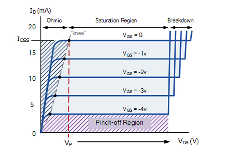
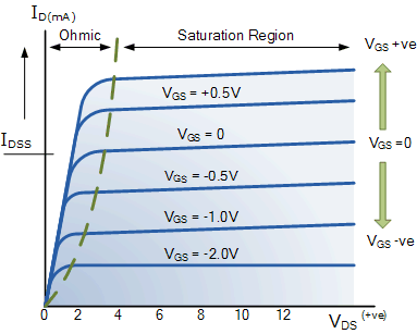
Operation modes
JFETs can only operate in depletion mode because of reverse biasing of its pn-junction. However, because a MOSFETs gate connection is completely isolated from the main current carrying channel, it can operate in both depletion and enhancement modes. This makes the MOSFET device especially useful as a logic gate because with no bias they are normally non-conducting and their high gate input resistance means that very little or no control current is needed.
Input impedance
Both devices have high input impedance, which is what makes them so great as switches. But again, because of its insulated gate, MOSFETs have a much greater input impedance (~10^10 to 10^15Ω) than a JFET (~10^8Ω). This is another reason MOSFETs are more useful as a digital switch than a JFET.
Damage resistance
But for the very same reason above, the almost infinite input impedance makes a MOSFET more prone to accumulating large amounts of static charge, and are therefore more prone to damage than JFETs, when not carefully handled or protected.
Output characteristics
Because the JFETs drain resistance is higher than that of a MOSFET, the output characteristics tend to be flatter than the MOSFET.
Cost
JFETs have a simpler, less sophisticated manufacturing process, making them cheaper to fabricate. However, MOSFETs are used more ubiquitously in the world of integrated circuits, making them easier to find and purchase on electronic component websites.
Form factor
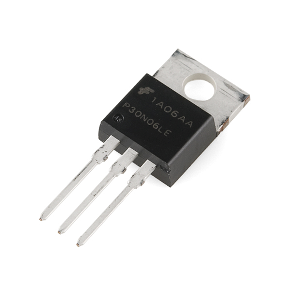
While their look may vary, both JFETs and MOSFETs will come as three-pronged devices. Many MOSFETs will have a drain pad, which gives them a characteristic “tab.”

General availability
You will find the world is full of MOSFETs — they are commonly used and have become a cornerstone of most integrated circuits. While the JFET has been around longer, it has been replaced in many of its original use cases by more modern devices like the CMOS OpAmp.
Resources
What’s the Difference Between JFET and MOSFET
Function Field Effect Transistor
The MOSFET
The formidable forgotten FETs
How about RF characteristics?