
High electron mobility transistors reduce power supply size thanks to special make-up that eliminates sources of energy loss.
Andrea Bricconi | Wei Deng, Infineon Technologies AG
It is an exciting time for power supply designers. We are learning how devices based on wide bandgap (WBG) materials such as silicon carbide (SiC) and gallium nitride-on-silicon (GaN-on-Si) open the door to new capabilities, often through new topologies.
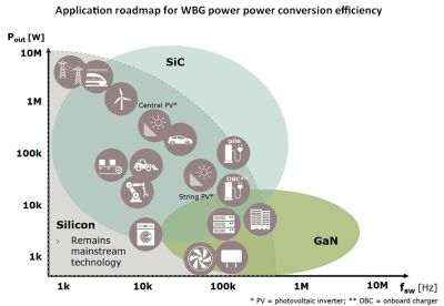
Broadly speaking, the advantages of both SiC and GaN-on-Si stem from lower on-resistance, the ability to operate at higher switching frequencies, and improvements in such important figures of merit as heat tolerance. The resulting advances in efficiency and lowering of losses bring higher power densities and better reliability in end products.
That said, silicon will continue to be a mainstream power technology, providing a good combination of power transmission and switching speeds. SiC is more suitable for higher voltages in the region of 600 V to 1.7 kV, at switching frequencies approaching 1 MHz. GaN-on-Si is excelling at switching voltages between 100 and 600 V at frequencies far in excess of 1 MHz.
One major difference between these two WBG materials is that transistor structures (i.e., MOSFETs, diodes, etc.) based on SiC resemble those for silicon. With GaN-on-Si, we can fabricate high electron mobility transistors (HEMT) that bring new advantages for power electronics. HEMT structures are significantly different than traditional MOSFETs, and it is worthwhile to explore the basis for this new structure.
A material’s bandgap is fundamental to its ability to carry a charge. The bandgap refers to the difference in energy between the valence band and conduction band (hence bandgap), between which electrons must pass during current flow. It is effectively the property that determines whether a material is a conductor, insulator, or semiconductor. Bandgap is measured in units of electron volts (eV), where a smaller number indicates a smaller gap and a better conductor. Semiconductor materials including silicon have a bandgap of between 1 and 4 eV, while a bandgap above 4 eV would typically indicate the material is an insulator.
While silicon is a narrow bandgap material with an eV of just over 1, WBG materials such as SiC and GaN have an eV of between 2 and 4. This gives them advantages over silicon semiconductors that can be exploited for power conversion applications. The mobility and abundance of charge carriers also determine the semiconductor properties of a material. (As a quick review, charge carrier mobility is the speed at which the charge carriers move in the material in a given direction, in the presence of an applied electric field.) If there is a great abundance of charge carriers, the material will conduct well even if its charge carriers have low mobility. Conversely, if a material’s charge carriers exhibit high mobility, it can be a good conductor even if there are relatively few charge carriers present. In this respect, the wide bandgap GaN matched with a narrow-bandgap silicon substrate is an ideal platform for transistors with a high level of electron mobility, hence the term HEMT.
Delivering HEMTs
One of the main structural differences between MOSFETs and HEMTs involves the direction of current flow. In a MOSFET, the charge carriers predominantly flow vertically. In HEMTs, such as the Infineon CoolGaN series, the charge carriers flow laterally. The direction of flow is due to the way the underlying silicon substrate interacts with the upper GaN layer. This interface is where much of the design innovation has happened in recent years, allowing GaN-on-Si to become a production-ready, high volume solution.
The CoolGaN fabrication process involves epitaxial growth of the transition layers on the silicon substrate to provide an efficient interface between the dissimilar crystalline lattice structures of silicon and GaN. This special interface overcomes the issue of an otherwise mismatched thermal expansion coefficient between the two materials. Further layers are deposited over the transition layers, including p-doped GaN, to form the transistor structure. Metallization and passivation steps complete the structure.
The addition of a p-doped gate results in a higher threshold voltage, effectively making the device a normally-off enhancement mode transistor. This feature can render the device sensitive to gate over-voltage, an issue overcome by developing a self-clamping p-type gate structure.

The GaN-on-Si HEMT has a conduction path that joins the drain and source, formed by the heterojunction created between the GaN and AlGaN layers. This bidirectional current path, referred to as the two-dimensional electron gas, or 2DEG path, is controlled by the gate potential which, as explained earlier, is held high enough to make the device normally-off and operate in enhancement mode, the preferred format for power electronics.
The HEMT structure of the CoolGaN series delivers several key benefits over the super junction MOSFETs commonly used in power applications. First, they are inherently more immune to the effects of temperature. This temperature tolerance brings a lower temperature coefficient of the on-resistance, RDS(ON). A lower temperature coefficient – around 2.0 for GaN-on-Si vs. 2.4 for silicon – reduces the conduction loss, which also contributes to the ability to operate at higher voltages.
As mentioned earlier, GaN-on-Si HEMTs can switch at higher frequencies than MOSFETs based on silicon or SiC. The reason is GaN-on-Si HEMTs lack an intrinsic body diode between the drain and source. The absence of a body diode is fundamental to what is probably the most important feature of GaN-on-Si, which is their vastly better reverse-recovery performance.
In other transistor structures, a body diode significantly limits switching performance. The effect of a body diode in other forms of transistors results in a reverse recovery charge which has with it a peak current. Reverse recovery charge is the charge that accumulates in the PN junction of a MOSFET’s forward biased body diode. In most applications, current flows through the body diode twice for each switching cycle, causing charge to build up. Peak current in topologies that feature repetitive reverse recovery becomes inhibiting.
The absence of a body diode and its associated reverse recovery charge and peak current is essential to the high- frequency operation of GaN-on-Si HEMTs. The ability to operate at high frequencies, in turn, allows them to make new switching topologies practical as well as play a role in half-bridge converters.
Furthermore, device output capacitance largely controls the rate-of-change of the voltage across the transistor, VDS. Superjunction MOSFETs based on silicon have an output capacitance that is highly non-linear. Initially, voltage changes slowly and then exhibits accelerated change before reverting to a slower rate of change as it approaches its working maximum. In a GaN-on-Si HEMT, the output capacitance is nearly linear with a variance that is around a tenth of that seen in superjunction silicon power transistors. This linearity also contributes to the higher switching performance of GaN-on-Si.
A direct result of this faster switching in conversion topologies is a reduced dead-time; the time between the change in the conduction path in a half-bridge configuration. Dead-time is an essential safety feature in converter topologies to avoid short-circuits between the two power rails. No conduction takes place during this time, which lowers the converter’s efficiency. In other types of transistors that cannot switch as quickly, the dead-time must be carefully calculated to avoid short-circuits. Because GaN-on-Si HEMTs switch faster, the dead-time can be shorter, boosting overall performance.
Also important is the overall system solution. Conventionally, the size of the passive components in a switching topology scale down with higher switching frequency. GaN-on-Si HEMT operating at higher frequencies can use smaller passive components, increasing the power density. The resulting footprint is smaller than an equivalent silicon MOSFET design. Better power density is perhaps the single most consistent demand in power conversion. GaN-on-Si HEMTs will bring power conversion that makes possible smaller end devices requiring less energy.
Sustainability is also important and is driving the development of more efficient solutions based on SiC and GaN-on-Si. All in all, Infineon CoolGaN technology, complemented by Superjunction MOSFET CoolMOS and CoolSiC solutions, make up a complete portfolio of power semiconductors for every application.


Leave a Reply