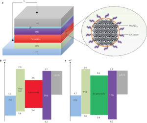
Engineering researchers at Princeton University say they have developed a technique for making LEDs in which nanoscale perovskite particles self-assemble themselves. The advance, reported Jan. 16 in Nature Photonics, could make perovskites a potential lower-cost alternative to gallium nitride and other materials used in LED manufacturing.
Perovskite is better known as a potential replacement for silicon in solar panels rather than for LEDs. That’s because perovskite can be cheaper to manufacture while offering as much efficiency as some silicon-based solar cells. To make perovskite-based LEDs, hybrid organic-inorganic perovskite layers are fabricated by dissolving perovskite precursors in a solution containing a metal halide and an organic ammonium halide. This is a relatively cheap and simple process.
The resulting semiconductor films could emit light in vivid colors when used in LEDs. But the crystals forming the molecular structure of the films have been too large, which made them inefficient and unstable. “The inability to create uniform and bright nanoparticle perovskite films has limited their potential,” said Barry Rand, an assistant professor of electrical engineering and the Andlinger Center for Energy and the Environment at Princeton.
“Our new technique allows these nanoparticles to self-assemble to create ultra-fine grained films, an advance in fabrication that makes perovskite LEDs look more like a viable alternative to existing technologies,” Rand, the lead researcher, added.
Perovskite is a mineral originally discovered in the mid-1800s in Russia and named for the Russian mineralogist Lev Perovski. The term “perovskite” extends to a class of compounds that share the crystalline structure of Perovski’s mineral, a distinct combination of cuboid and diamond shapes.

In their new paper, Rand and his team report that the use of an additional type of organic ammonium halide, and in particular a long-chain ammonium halide, to the perovskite solution during production dramatically constrained the formation of crystals in the film. The resulting crystallites were much smaller (around 5-10 nm across) than those generated with previous methods, and the halide perovskite films were far thinner and smoother.
This led to better external quantum efficiency, meaning the LEDs emitted more photons per number of electrons entering the device. The films were also more stable than those produced by other methods.
Russell Holmes, a professor of materials science and engineering at the University of Minnesota, said the Princeton research brings perovskite-based LEDs closer to commercialization. “Their ability to control the processing of the perovskite generated ultra-flat, nanocrystalline thin films suitable for high-efficiency devices,” said Holmes, who was not involved in the research. “This elegant and general processing scheme will likely have broad application to other perovskite active materials and device platforms.”
Other authors on the paper were Princeton researchers Zhengguo Xiao, Ross A. Kerner, Lianfeng Zhao, Kyung Min Lee, and Tae-Wook Koh of the electrical engineering department, and Gregory D. Scholes and Nhu L. Tran of the chemistry department.


Leave a Reply