
OK, so maybe it’s not the logical follow-on from the buck converter but nevertheless a useful converter and probably a bit more interesting than the boost converter. The SEPIC – Single Ended Primary Inductance Converter – is useful because while a buck converter allows you to step down the voltage and a boost converter allows you to step up the voltage, a SEPIC can do either. So, if your input voltage has a range of 6V to 12V and you want a 9V output, you need a SEPIC. If you wanted -9V then a simpler converter, the flyback, could be used but if both input and output voltages are in the same polarity then you need a SEPIC.
There are some good descriptions around such as the Texas Instruments documents slyt309.pdf or snva168e.pdf (AN-1484) so I won’t duplicate that – just try to give a simple summary. Read those application notes while using a simulator to help understand the converters. As an example, the diagram below shows a typical SEPIC with a coupled inductor using the Linear Technology LT3467A which can be simulated with the free LTspice software.
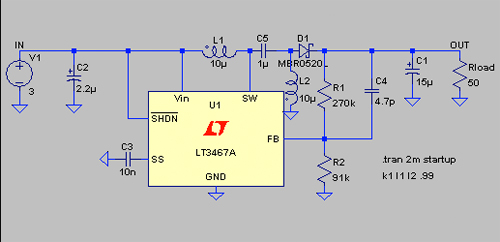
The example circuit shown above uses coupled inductors. The SPICE directive “k1 l1 l2 .99” is what links the two inductors with a coupling factor, K, of 0.99. While a SEPIC can use two separate inductors, there are cheap, coupled inductors around which help reduce the footprint of the finished PCB. For example, the Coilcraft LPD4012 surface mount coupled inductors are only 1.1mm thick and 4mm square but have around 1A saturation current for the 10uH version.
One important difference between the SEPIC and buck or boost converters is the presence of the series capacitor, C5 in the diagram above. This gets charged up to the input voltage – imagine the voltage across it when the regulator chip switch (pin SW) is OFF and that is where the voltage across C5 stays because the average voltage across each of the inductors must be zero (otherwise the current would theoretically keep on increasing to infinity with time).
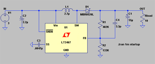
One way of viewing a SEPIC is that L1 and the switch and diode form a BOOST converter but with C5 allowing a voltage drop. The DC path between the input and output of a boost converter prevents the output voltage being lower than the input voltage. The voltage at the switch (SW) is Vin+Vout when the switch is off and zero when the switch is on. For comparison purposes, this is what a boost converter looks like:
If you plot the current in both the inductors and the capacitor C5 in the SEPIC you will see that the capacitor is supplying the current to L2 when the switch is on, and receiving current from L1 when the switch is off:

L2 current is shown inverted so the sign is correct for overlaying the capacitor current. Because the traces overlay it is tricky to see them so here are the same traces but separated:
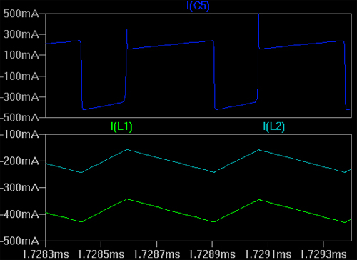
These traces are with a 200mA load current at 5V and 3V input voltage. Using the free LTspice you can experiment with the input and output voltages, load resistance and component values while probing the voltages and currents in the circuit to see how it works. Also, remember to look at how the duty cycle changes – it is the only way the control IC can maintain the output voltage with varying loads and input voltages. You can do all this without blowing up any devices which makes simulation a powerful tool and learning aid. Then, compare what you see with the calculations in the various applications notes, such as the ones mentioned above.
Leave a Reply