by Leland Teschler, Executive Editor
Manufacturers are making 3D-printed electronics a reality even for designs involving sophisticated multi-layer circuit boards.
The sun is starting to set on the days of cobbling together prototype circuits with wires and perfboards. Increasingly, new ideas for electronics will take shape on substrates fabricated by desktop machines taking cues from ink-jet 3D printers.
And 3D-printed electronics isn’t just for maker-movement hobbyists tinkering on home projects. There are machines on the market and on the drawing board able to produce sophisticated PCBs having multiple layers, complete with passive components fabbed with the same conductive inks and dielectrics used to make circuit traces. Manufacturers say even film-based transistors and diodes can be fabricated with some of the 3D-circuit printing equipment now on the market.

Nevertheless, the market for 3D printed electronics equipment is tiny. According to Jon Harrop, director of the IDTechEx market research firm, the 3D-printed electronics market is worth around $20 million today, slightly less than what the New York Yankees paid designated hitter Alex Rodriquez to play baseball in 2015. Harrop estimates that figure (the market size, not A-Rod’s salary) will grow to at least a billion dollars in ten years. “I say ‘at least’ because I have forecast what we know, but I expect things I do not yet know will make that number much bigger in practice,” he said. “For example, 3D-printed electronics is an ideal solution for many of the problems in huge emerging markets such as wearable technologies and structural electronics. But it is too early to tell how big a slice of those pies will end up being printed.”
Interestingly, the big names in 3D printing don’t seem to be making any noise about printed electronics. None have announced products in the field. “Stratasys particularly is in a great position (for printed electronics) as it dominates the multimaterial 3D printing market. I have also heard that Stratasys has demand from its existing customers but nobody knows of any work they are doing on it,” said Harrop. “As far as I know, 3D Systems is doing nothing in this regard. I believe Hewlett-Packard has demonstrated 3D printing of conductive and insulating materials together using its Multi Jet Fusion technology, but I expect HP will focus on the larger traditional mechanical markets, at least to begin with.”
The companies making most of the headlines in printed electronics tend to get their start on Kickstarter. That is the case for companies that include AgIC, Voltera, Cartesian Co. and BotFactory. These firms are fielding technology that concentrates on printed circuit boards created either by hobbyists or by engineers interested in seeing a single prototype. In addition, Optomec and Nano Dimension have machines that can handle PCBs but also more sophisticated tasks such as printing electronics on three-dimensional surfaces, or on boards having a dozen layers or more.
But many observers say the best is yet to come in printed electronics. “I think a hybrid CNC machine that combines the pick-and-place capabilities offered by BotFactory’s Squink with the high precision and multilayer capabilities offered by Nano Dimension and the fully 3D capabilities offered by Voxel8 would be a killer solution and sell like hot cakes,” said Harrop.
PCBs for nudniks
The majority of Kickstarter machines that print PCBs have several elements in common. Most convert ordinary Gerber files for PCB layouts, or common graphic files, to a form compatible with ink jet printing. Most also use commercially available ink jet print heads. The print heads squirt out ink in the usual fashion, but the ink is engineered to have either conductive or electrical dielectric properties. The deposited inks typically undergo a curing step consisting of a heat treatment. This usually takes place on the bed of the printer.
Many Kickstarter machines produce boards on what might be called flimsy substrates such as coated paper or thin plastic. So the heat during the curing process has to be kept relatively low, typically lower than the heat deflection point for common plastics. For the relatively small PCBs that these machines produce, it might take 15 to 20 minutes to print out traces, then another half hour to cure the board.
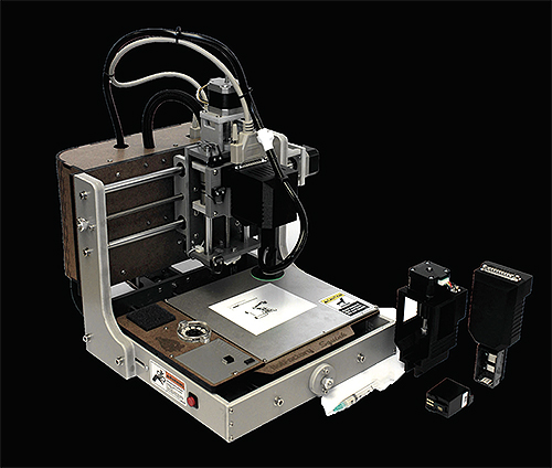
For an example of a printer in this category, consider the Voltera V-One. Rather than using ink jets, it employs a paste deposition system to extrude paste through a nozzle. It can deposit 8-mil traces with a pin-to-pin pitch of 0.8 mm on a print area of 5.5 x 4 in. The typical board material is ordinary FR4, but Voltera co-founder Jesus Zozaya said the firm has successfully run boards on polyamide and PET. The V-One has a single print head. So the process of printing a board involves plugging in the cartridge containing conductive paste, laying down traces, swapping out the cartridge for one containing dielectric, then dispensing an insulating layer.
The V-One accomplishes the printing of two-layer circuits by sandwiching an insulating layer between layers of conductive pastes. Software automatically converts vias in the PCB design into bridges so that one trace can jump over another. With the insulative jumpers in place, another pass with the conductive cartridge creates the bridges comprising the second layer. Then the board cures at an elevated temperature. Voltera also said it plans to scale the technique for higher layer counts later on.
A third cartridge can be swapped in to dispense solder paste. The solder paste module can work on boards made with traditional etching methods, and these boards can be reflow soldered on the print bed thanks to the 550-W heater it contains.
Zozaya said boards from the printer have handled 16-MHz clocks so far, though the upper limits on clock speed haven’t been tested. “Trace resistance is quite good,” he said. “We expect a small trace to be only one or two ohms.” To create wide traces for handling higher current, the printer makes multiple passes, building up a wide trace from multiple 8-mil-wide depositions.
The V-One is in “pre order” status, so those interested in obtaining one of the $2,200 PCB printers will probably be able to get their hands on one in February or thereafter.
Pick and place
The approach taken by BotFactory with its Squink PCB printer is a combo PCB printer/pick-and-place machine for SMD circuits. After the Squink is finished putting down traces, it uses the solder mask file to place dots of conductive glue or solder paste in every connection point where a part will sit. Squink uses the “centroid and rotation” file created in a CAD tool to figure out where and how to place board components. With a vacuum tool, it picks components from a tray, corrects alignment and rotation, and uses onboard computer vision to place components in the correct spot. Each component is picked from a tray, not a rail, to keep the setup simple.

The Squink uses two X-Y stages for positioning, one for the print head, the other for moving the PCB platform. A single tool head handles both circuit printing and SMD placement. The first head deposits the conductive ink on the PCB. The operator then swaps the conductive ink cartridge for a conductive glue dispenser. Once the glue is in place, a vacuum pick-up assembly gets swapped in to pick-and-place components. There’s an optional 15-minute heat-curing cycle to set the glue.
The Squink takes about a half-hour to fabricate printed circuits and place components on a board up to 5 x 5 in. PCB substrates can be photo paper or coated transparency film. BotFactory CTO Carlos Ospina said the firm is developing inks for glass, plastic and Kapton film, and FR4 board material. “Squink is a connected device, complete with an onboard computer that is updated at least twice a month. For users, this means Squink is constantly improving, optimizing its UX/UI, learning new components, footprints, and incorporating feedback from our existing community of users,” he said.
Ospina also said BotFactory developers have run boards made with Squink up to 400 MHz without seeing any signal degradation. But microwave-style waveguide PCB patterns are probably not feasible, he explained, because they involve traces with varying widths, something the Squink can’t handle. And at really high frequencies, ripples and bumps in the traces become a problem. So for high-frequency applications, Ospina thinks Squink users will probably start with a standard bare board made by conventional means, then use the Squink to apply paste and populate components.
The Squink is for single-layer designs and doesn’t handle through-holes. Its minimum trace width is 10 mil with 15 mil spacing, possibly too coarse for some high-density IC packages.
The Squink costs $3,000 but with almost immediate gratification; lead time is listed as one week.
A ten-layer printed PCB
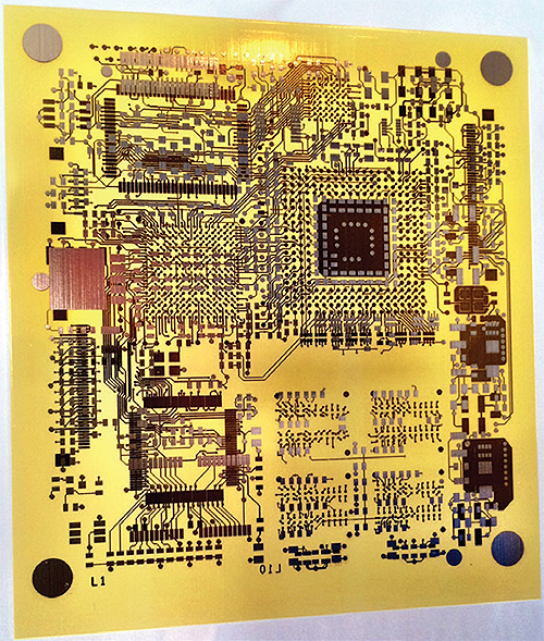
Not all PCB printers cater to simple board designs. The Dragonfly 2020 from Nano Dimension in Israel will be optimized specifically to fabricate multiple-layer boards when it comes out sometime in 2016. “We wouldn’t launch the machine without the ability to print at least 12 layers,” said Nano Dimension Co-founder Simon Fried. “We expect it to be able to handle 20 layers and we wouldn’t be surprised if our first units could print 30 layers or more.”

Nano Dimension is also aiming for a design able to do 3.5-mil trace widths and a similar pitch, finer than what’s available from single and two-layer PCB printers. The Dragonfly also has a bigger print bed, 20 × 20 cm., or almost 8 in. on a side. And precision isn’t its only virtue. “Stuff that’s tough to do conventionally isn’t tough to do with our additive process,” said Fried. “If you want a via that leans at 45°, the Dragonfly is happy to print it. You can put geometries on the board that otherwise couldn’t be manufactured at all.”
Though Dragonfly-printed boards may contain interesting geometries, Nano Dimension expects their frequency response to mimic that of boards manufactured with conventional etching, said Fried. “Academic research so far indicates they should deliver good high-frequency response because of the way materials are laid down. You don’t have the jaggedness of the edges that’s present with regular etching, for example. To conventionally plate copper on an FR4 board, the board needs a certain amount of roughness so the copper adheres. You don’t get this roughness with a printed board,” he said.
Unfortunately, many of the Dragonfly’s details are still under wraps. The print heads are high-resolution industrial units purchased from a vendor. The rest of the design, and particularly the formulation of the inks, all takes place in house. “The printer contains a lot of secret sauce as it integrates several high-end technologies. The resolution of the mechanics is in the low microns. The ink chemistry is complex and the ink, print-head management, and control all interrelate,” said Fried.
For example, the dielectric material used is specially formulated to match the material properties of the FR4 substrates widely used in the PCB industry. “It is a type of epoxy like that created when a resin and hardener mix. We created a one-part epoxy liquid containing the resin and hardener fashioned so the resin and hardener can’t mix until they print. We also add other materials to adjust properties such as the mechanical strength,” said Fried.
Fried said the parameters of the printers are such that they can be adjusted to consider future requirements such as the ability to operate at higher frequencies or to dissipate heat. “For example, you can make the dielectric look more like Teflon if you want something that’s good at higher frequencies,” he said. He also said the company expects to be able to print flex circuits in the foreseeable future.
“We wanted to make sure our boards can be reflow soldered. The dielectric material we use comfortably supports temperatures of 300° C without warping, twisting, melting or changing in any way. High-end reflow ovens operate at about 270° C, so our boards can handle reflow and hand soldering,” said Fried.
Also on the development road map are super-thin traces and even passive components fabricated on or within the board along with the conductive traces. “In lab conditions we are getting down to 60-µm-wide traces without changing print heads. If we change heads you might be capable of printing 15- or 20-µm lines,” said Fried. “The printing of passive components is on our road map. We are working with a university in Singapore to do this. It isn’t trivial, but it is doable. You can put down a minimum thickness of about 2 µm to make, say, noise-reducing capacitance built right on the board. But passive component capability won’t be part of the first printer because it requires a different print head.”
The first Dragonfly printers are now in beta testing and will produce multilayer boards that “will mimic what you would get in a regular prototype multilayer PCB in terms of going through reflow and in trace conductivity. They should also work fine for one-off situations,” Fried said. Deliveries will start in the latter half of 2016 and the machines will be in the $50,000 range.
Mass production meets printed electronics
Optomec takes an approach to printing electronics that is quite different than that of other firms. Most other printer makers buy print heads from vendors and engineer their inks and hardware around them. In contrast, Optomec designs its own print heads using a technology it dubs Aerosol Jet. But this approach lets the printer use a variety of commercial inks from various suppliers, so printer users aren’t tied into a single ink supplier.

Additionally, the Optomec print heads are offered in the form of print engine assemblies. The assemblies can be built into conventional automation equipment such as CNC positioners or special-purpose motion control systems. Several print engines can be combined to print simultaneously as for mass production settings. Optomec uses an open systems approach for deploying the print heads, so automation suppliers can integrate Optomec gear into numerous kinds of production settings. Optomec said it has sold about 130 of the Aerosol Jet systems.
The claim to fame of Aerosol Jet printing is super high resolution and control of the inks. The print engines can create features as small as 10 µm wide and make deposits with thicknesses measured in nanometers. Conversely, the same print head can make features that are several millimeters wide and several microns thick. And features at both extremes can be printed in the same pass.
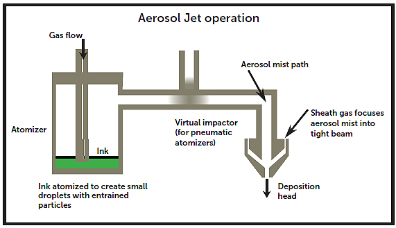
The Aerosol Jet system accomplishes this sort of precision because it is different from conventional ink jetting. Ordinary ink jets depend on gravity to bring ink drops to a substrate. The drops spread out or widen as they fly from the nozzle to the substrate. In contrast, Aerosol Jets created a more tightly focused beam of ink by first atomizing the ink supply into a mist, then shooting the mist through the deposition head while simultaneously surrounding it with a flow of inert gas. This so-called sheath gas both speeds up the flow of the atomized ink as it traverses between the head and the substrate and behaves as a focusing mechanism for the atomized ink stream. The result: From print nozzles having 100-µm diameters come 10-µm-diameter collimated streams of atomized ink.

The atomizing process can use either ultrasonics or pneumatics, depending on the kind of ink involved. The resulting mist droplets are 2 to 5 µm in diameter and contain numerous nanoparticles of ink. (If pneumatic atomization is used, there is a densifying step that removes some of the gas from the atomized stream before the atomized ink gets to the print head.) The sheath gas accelerates the mist to a point where it is moving at 50 m/sec when it emerges from the print head.
The relatively high exit velocity lets the mist stay collimated over at least a 5-mm distance between the print head and substrate. What’s interesting about this facet of performance is that the mist can remain focused while hitting nonuniform surfaces. This ability to navigate over uneven terrain lets the printers deposit features on three-dimensional parts.
The ability to print high-resolution conductive and dielectric layers on 3D surfaces makes the Optomec printers candidates for a variety of applications. “Areas of focus for us right now are printed sensors and printed antennas,” said Optomec VP of Marketing Ken Vartanian. “We have printed 3D sensors on turbine blades that measure how the blade expands over its life. That is a particularly noteworthy application because the inks on the blades must withstand 1,800° F without deteriorating. We’ve also printed connections on integrated circuits that replace wire bonding and conventional die-stack attachment techniques.”

Vartanian said the Aerosol Jet process has been built into production machines making 3D antennas and can be a more green manufacturing method than traditional alternatives that involve copper plating. In one case, Aerosol Jet printing is used to make conformal antennas that formerly required laser direct structuring on injection molded parts. Aerosol Jet printing is viewed as superior in that case because it eliminates nickel and copper plating processes.
Likewise, Aerosol Jet printers are now used to fix gaps in conductors on flat-panel glass displays and to perform similar functions on solar panels. Researchers at the University of Minnesota and University of Massachusetts are also employing the printers to deposit semiconductor material and more exotic conductors to realize thin-film transistors and diodes.
The Aerosol Jet system is built to stand up in high-volume production settings. The cost of the print engine itself depends on the number of print heads and other attachments and is in the $150,000 ballpark. Though OEMs can get these print engines and build them into automation equipment, Optomec also offers the print heads in stand-alone benchtop systems that start at around $200,000 and as part of a five-axis machine for around $500,000 designed for more complex development work.


Is it possible to develop not only PCBs but ICs itself, print transistors, gates, flip-flops?