
IGBTs have nuanced operations associated with high current densities and temperature that force IGBT gate drivers to incorporate sophisticated features.
Tom Zemites, Kim Gauen, NXP
The automotive industry is moving inexorably towards electrification. As automakers move from electric assistance to full autonomy, the trend in EV invertors is toward higher system efficiency and functional safety using technology that also lowers costs.
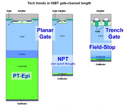
A key consideration in the EV inverter market is the need for smaller and less expensive IGBT modules to help lower costs. Consequently, the industry is moving to boost IGBT current density by shrinking the length of the gate channel. The shorter channel facilitates reduced IGBT die size while lowering forward voltage drop. Smaller die size makes for smaller modules that cost less. Lower forward voltage drop will reduce IGBT power dissipation by nearly 15%. With smaller modules, lower cost, with increase efficiency, we have the perfect trifecta. What could be wrong with this picture?
The trade-off for IGBTs having a high current density is a greater energy density when conducting overcurrents or during short circuits. The greater energy density can quickly stress, if not destroy, an expensive IGBT module. It becomes necessary to quickly sense the overcurrent condition, make the correct assessment, and softly shutdown the IGBT.
There are four key requirements for an ideal gate driver integrated circuit (GDIC). They include being able to minimize system cost, minimize PCB area, ensure the system meets ISO 26262 requirements, and design flexibility for re-use.
Minimizing system cost
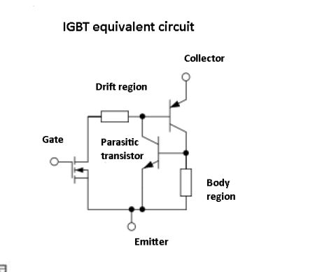
It may be useful to review the major differences between IGBTs and MOSFETs because some of these differences dictate the functions a GDIC must provide. First, IGBTs and MOSFETs are both controlled via an isolated gate and both behave similarly. However, IGBTs use minority carriers to conduct current whereas MOSFETs are majority carrier devices. Use of minority carriers allows IGBTs to support a high current density.
However, IGBTs have a more complicated structure than MOSFETs. They have a stored charge that creates a turn-off tail and some accompanying losses. IGBT switching behaviour also changes with junction temperature. An IGBT is more prone to latch-up because it has a four-layer structure, and this may also restrict the device safe operating area. IGBTs have a higher gain than do MOSFETS, resulting in more short-circuit current for a given gate voltage. Similarly, IGBT power density is greater during a short-circuit fault. Finally, ordinary IGBTs lack an integrated body diode (though new “reverse conduction” IGBTs do have one).

With these factors in mind, one can understand how a GDIC can help minimize EV inverter cost. In the newest generation IGBTs, the magnitude of fault current rises as the current density increases. This mandates that the newest generation IGBTs integrate ISENSE outputs enabling quick sense of an overcurrent condition. The GDIC can improve short circuit protection by monitoring the IGBT ISENSE pin and provide quick detection (less than 2 µsec) and shutdown during an overcurrent episode. The GDIC implements two-level turn-off to reduce gate voltage during a fault detection, thereby reducing the peak fault current. (As a quick review, a short-circuit or over-current in the load can cause a large voltage overshoot across the IGBT at turn-off that can exceed the IGBT breakdown voltage. By reducing the gate voltage before turnoff, a two-level turn-of limits IGBT current and reduces the potential over-voltage.) Soft shutdown can be used to gently turn-off the gate voltage once the fault is validated.
The GDIC can also lower the heat the IGBT and the printed circuit board (PCB) radiate by boosting overall inverter efficiency. One efficiency boosting measure is to integrate gate-driver transistors within the GDIC. This not only reduces component cost and PCB area, it also provides direct and independent control of the charging and discharging paths. This also minimizes the delay before protection kicks in and allows for a close monitoring of the gate voltage.
Rail-to-rail control can be used to determine on-state voltage. Off-state voltage is pulled to the negative supply and not to a diode drop above it. A GDIC can also implement an active Miller Clamp (AMC) feature which minimizes system cost in several ways. (Again, as a quick review, turn-on or turn-off of an IGBT can cause high dvCE/dt. Displacement currents flow through the IGBT parasitic capacitances and may unintentionally turn-on the IGBT. A Miller clamp sinks the Miller current across a low impedance path in this high dv/dt situation.)
A dedicated AMC pin allows designers to omit the negative gate drive supply that is otherwise often needed. Omitting the negative supply saves PCB area while eliminating a few components. More importantly it eliminates the gate drive losses (an estimated 35% extra gate power) associated with a negative supply. The result is less heat on the gate drive board and a gate-driver power supply smaller than would otherwise be needed.
Another way a GDIC can shrink PCB area is by integrating several features that ordinarily might require several separate circuit elements. For example, the GDIC might incorporate the high-voltage galvanic isolation. It might also incorporate less obvious features like post regulation of the gate power supply, so power supply outputs can be combined into fewer transformer cores, reducing the number of components that span the galvanic isolation barrier. If the ISENSE pin is available on the IGBT, there’s less need for Vce active clamping to address failure modes associated with high di/dt, high dv/dt, gate-emitter and collector-emitter over voltages. Thus, there’s no need for active-clamping zeners and associated diodes.
Meeting ISO 26262 ASIL-D metrics
ISO 26262 safety compliance is an emerging standard that will likely be required for most EV inverter systems. ISO 26262 entails a strict design and documentation process that ensures products meet stringent safety demands. A GDIC can offer features that simplify the process of meeting safety compliance specs. These features include safe SPI (serial peripheral interface) configurable mode, framing error detection, IGBT on/off state validation, continuous monitoring of power supplies, and interface pins for low-side and high-side safety logic.
Pins such as AMUXIN and AOUT provide a duty cycle-encoded signal to represent the IGBT temperature, GDIC temperature, gate supply voltage and an axillary AUMXIN monitor. This feature eliminates the need for external feedback from the HV domain.

The final requirement for an ideal gate driver IC is design flexibility and reuse. The type, generation, size, pinout and features of IGBTs vary widely. So, the response of the GDIC must be tuned to optimize the performance of a given IGBT. By including an SPI, extensive programmability of the GDIC allows optimization of IGBT operation regardless of the specific IGBT chosen. The GDIC can set features such as short circuit and over current levels, over temperature warning and over temperature shutdown, gate supply under-voltage shutdown threshold and filters. Moreover, the GDIC can help realize PWM deadtime, different operating modes, Vge monitoring, two-level turn-off voltage and time control.
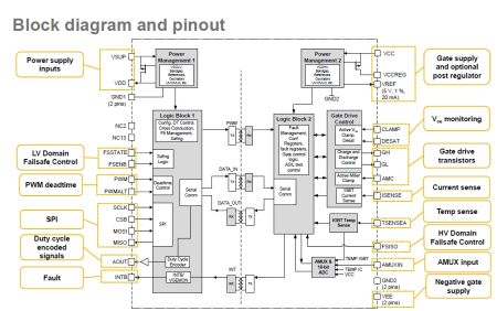
NXP offers an advanced gate driver for high-voltage power IGBTs which integrates the high-voltage isolator. The MC33GD3100 device offers current and temperature-sense features, including integrated current and temperature-monitoring outputs, that work directly with the new high-current-density IGBT modules. This gate driver provides quick detection of an over-current event as is necessary to minimize stress on IGBTs resulting from short circuits. Its integrated high-voltage electrical isolation between the low-voltage drive electronics and the high-voltage power electronics allow for communication between isolated and non-isolated domains. Its protection and diagnostics features are programmable, and it is compatible with fail-safe management from either the low-voltage or high-voltage domains.
On the MC33GD3100, the SPI interface for ASIL C/D monitoring and reporting provides detailed fault and status data to meet ISO 26262 requirements. The GD3100 is also compatible with IGBTs that do not have a current and temperature sense pin; in this case it will monitor a collector-emitter voltage and provide desaturation threshold shutdown and clamping.
All in all, the gate driver remains a key element connecting the power domain to the control domain and helps to drive higher system integration and lower design costs.

Leave a Reply