(editor’s note: Intrigued by these power electronics problems? Have a question or another solution? Then click the “Read more” link and follow the conversation on EDAboard.com or log in to EDAboard and participate in the power electronics forum thread.)
Help with step down 48V to 12V – I want to convert from 48V to 12V using a DC/DC converter. I found a lot of things on Internet but the circuit I made is getting 65% efficiency and it sounds bad. The original circuit is from Roman Black and I am open to suggestions of new projects, the only change I made was replacing the original transistor from a BC327 to a TIP127, yes I know TIP127 is very slow and I do think that’s the problem, but since I will work with about 0.6A, I needed a Darlington transistor. Read more
High-frequency 60kHz converter circuit – I wanted to build a circuit that can use 24V DC and converter to AC @800V at about 60 kHz any waveform is acceptable. I was wondering if anyone knew of any working circuits I could try out in a similar range. Read more
Boost Converter: current oscillation problems – I’m using a boost converter at a 15 kHz Switching frequency. I’m using a coupled inductor with a value of 2 X 1600 µH. I’m using an IGBT module where I am switching the bottom IGBT and the top IGBT is used as a diode (the reverse protection diode). The problem is that I’m having oscillations in the current during the switches. Read more
Induction heating for aluminum and copper – I am building an induction heating system without current and voltage feedback. Now I am looking to be able to melt copper and aluminum by induction heating but these materials are less responsive than iron because they have lower resistance than iron. What is a suitable resonant frequency and design of induction heating for aluminum and copper melting? What is a suitable method for current and voltage feedback for induction heating? Read more
Flyback transformer design – I have designed a transformer for flyback converter(100-150V in, 3 outputs for 35W total). I am listing all specs. Is it okay? Read more
Phase–shifted full bridge, ringing, EMI – I’m working on a phase-shifted, full-bridge DC/DC power supply prototype. The converter has been designed for 800W continuous power and must regulate for max 2 seconds of 2400W overload. The input is 400V coming from external power supply for now (later from PFC) and the output is 170V in a complementary fashion (+85V/-85V). My problem right now is the ringing on the input side of the converter due to the discontinuous nature of input current in full bridge converter. Read more
Switching frequency for the DC/DC converter – What is the highest switching frequency for the DC/DC converter from 12V to 1V@15A? I am applying for the job position in and have discussed the issue with Dr. Shuming Xu, CTO in the company. He claimed the latest answer is 4meg HZ and 94% efficiency. Frankly it is beyond my experience. In my opinion 500K HZ is the highest switching frequency for this spec. Would you please share your experience/opinion? Read more
Desirable Vout ripple – What is a good value for “desirable voltage ripple” on the output of a SMPS powering a high-power LED?
Cout (min) = ΔI / 8 • Fsw • ΔV.
Cout (min) = 0.115 / 8 • 0.09 • ____
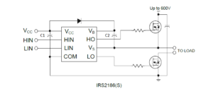
Problem with gate driver IC – I have been working with the gate drive IC IRS2186 and I have posted the recommended connections from the datasheet, with Vcc at 12V and the MOSFET high side voltage at 30V and 10µF for C2 and 1µF for C1. I can get the low side to work just fine but the high side HO always remains at 12V no matter what input. Ultimately I would like to increase the voltage to 170V though I thought a lower voltage test setup would help. Read more
Full-bridge inverter snubber design – I want to discuss snubber design/topology for a phase shifted full bridge adapted for an inverter (DC-1khz) application with about 30A output at ~750w. This is the basic topology with my current simple RC snubber shown:
So does anyone have general comments or suggestions for snubber design/topology in this application (or other comments on the desire to limit voltage at the secondary FETs). Note that the schematic as drawn also roughly represents planned layout. Read more


Leave a Reply